
A hemt switch device

A technology of switching devices and elastic parts, which is applied in the field of microelectronics, can solve the problems of large static power consumption and slow response speed, and achieve the effects of high power capacity, fast switching speed and high breakdown voltage

Active Publication Date: 2020-11-17
XIDIAN UNIV
View PDF7 Cites 0 Cited by
  • Summary
  • Abstract
  • Description
  • Claims
  • Application Information

AI Technical Summary

Problems solved by technology

[0004] However, there are few studies on HEMT switching devices at present, and the existing HEMT switching devices have slow response speed and large static power consumption.

Method used


Image

  • A hemt switch device
  • A hemt switch device
  • A hemt switch device

Examples


Embodiment 2

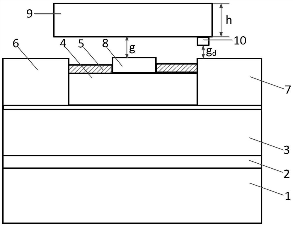
[0056] On the basis of the above-mentioned embodiments, this embodiment explains in detail the preparation process of the suspension electrode, which specifically includes the following steps:

[0057] S01, depositing a first LTO layer with a thickness of 100 nm on the source electrode 6, the gate electrode 8, the drain electrode 7 and the passivation layer 5;

[0058] S02. Etching a first groove with a depth of 100 nm at the position of the drain electrode 7 on the first LTO layer;

[0059] S03, continue to deposit a second LTO layer with a thickness of 100 nm on the first LTO layer, and a second groove corresponding to the position of the first groove will be formed on the second LTO layer;

[0060] S04, depositing metal W at the second groove to form bump electrodes 10;

[0061] S05. Deposit P-type doped Si with a thickness of 1 μm above the second layer of LTO and the bump electrode 10 0.4 Ge 0.6 As a suspension electrode 9;

[0062] S06, using 49% steam hydrofluoric a...


PUM

PropertyMeasurementUnit
thicknessaaaaaaaaaa
thicknessaaaaaaaaaa
thicknessaaaaaaaaaa

Abstract

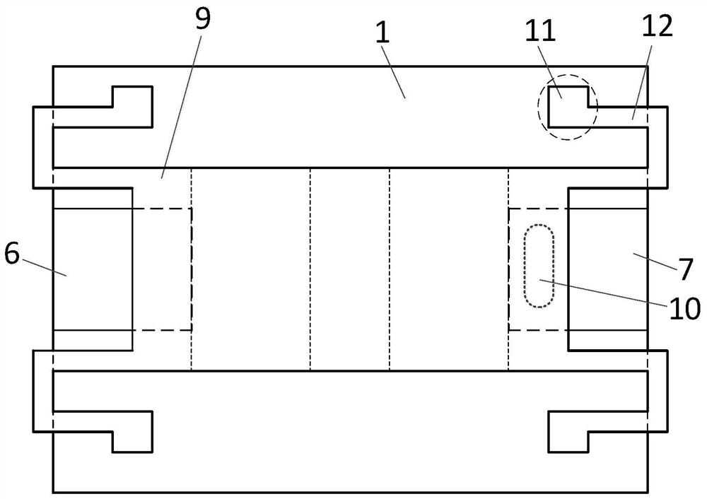
The invention discloses a HEMT switching device. The switching device comprises a suspension electrode (9) and a bottom structure, wherein the suspension electrode (9) is fixed above the bottom structure through an elastic part (12), and the suspension electrode (9) is provided with a salient point electrode (10) at the bottom; the bottom structure comprises a substrate (1), a nucleating layer (2), a buffer layer (3) and a barrier layer (4); in addition, the elastic part (12) is arranged on the substrate (1); a source electrode (6) and a drain electrode (7) are further arranged on the upper surface of the buffer layer (3); the drain electrode (7) corresponds to the salient point electrode (10); and a gate electrode (8) and a passivation layer (5) are arranged on the upper surface of the barrier layer (4). The HEMT switching device provide in the invention is extremely low in static power consumption and high in switching speed, and further has the characteristics of being high in breakdown voltage and large in power capacity.

Description

technical field [0001] The invention belongs to the technical field of microelectronics, and in particular relates to a HEMT switch device. Background technique [0002] Power electronics technology refers to the technology of transforming and controlling electric energy using power electronic devices. Power electronic devices, also known as power semiconductor devices, are the core components of power electronic systems. They are widely used in industrial equipment, household appliances, automotive power supplies, etc. Numerous areas. With the rapid development of power electronic technology, the new generation of power electronic devices requires higher efficiency, higher power density and higher reliability under high temperature working environment [0003] In the prior art, HEMT, that is, High Electron Mobility Transistor, is a kind of power electronic device, which has the characteristics of larger forbidden band width, higher critical breakdown electric field and str...

Claims


Application Information

Patent Timeline
Patent Type & Authority Patents(China)
IPC IPC(8): H01L29/778H01L29/423H01L21/28H01L21/335
CPCH01L21/28H01L29/42316H01L29/66462H01L29/7787
Inventor 郑雪峰陈轶昕王士辉李纲马晓华郝跃
Owner XIDIAN UNIV
Learn More