Novel hybrid photovoltaic cell and preparation method thereof

A photovoltaic cell and hybrid technology, applied in the field of new hybrid photovoltaic cells and their preparation, can solve the problems of no significant improvement in organic solar cells, environmental risks, and high manufacturing costs, achieve excellent photoelectric conversion efficiency, and improve cost. The effect of excellent film properties and electrical conductivity and electrical conductivity

Active Publication Date: 2019-02-15
新优(宁波)智能科技有限公司
View PDF12 Cites 0 Cited by
  • Summary
  • Abstract
  • Description
  • Claims
  • Application Information

AI Technical Summary

Problems solved by technology

The photoelectric conversion efficiency of monocrystalline silicon solar cells is very high, but in its production, it requires high-purity silicon wafers, a high-temperature annealing process up to 1000 degrees Celsius, an etching process with serious environmental pollution, and other complicated manufacturing processes, resulting in The manufacturing cost of this type of crystalline silicon battery is relatively high, and the manufacturing process also has environmental risks
With the development of the solar cell industry, organic solar cells are expected to reduce their production costs due to their advantages such as cheap materials, low annealing temperature, and simple manufacturing process. However, the efficiency of organic solar cells is much lower than that of monocrystalline silicon cells. With the development of time, organic solar cells still have no significant improvement and cannot replace conventional crystalline silicon solar cells.

Method used


Image

  • Novel hybrid photovoltaic cell and preparation method thereof

Examples


preparation example Construction

[0028] The present invention proposes a preparation method of a novel hybrid photovoltaic cell, comprising the following steps:

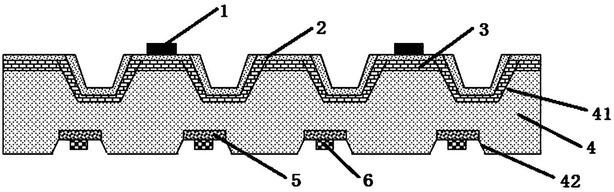
[0029] 1) An N-type silicon wafer is provided, the N-type silicon wafer is cleaned, and then a plurality of first grooves arranged in parallel and spaced apart are formed on the upper surface of the N-type silicon wafer, and then the N-type single crystal The lower surface of the silicon wafer forms a plurality of second grooves arranged in parallel and arranged at intervals. The second grooves correspond to each other one by one, and the first groove and the corresponding second groove partially overlap in the vertical direction, and the bottom surface of the first groove and the corresponding second groove The thickness between the bottom surfaces of the grooves is 100-200 microns, and the width of the overlapping portion of the bottom surface of the first groove and the bottom surface of the corresponding second groove in the vertical direction i...

Embodiment 1

[0044] A method for preparing a novel hybrid photovoltaic cell, comprising the following steps:

[0045] 1) An N-type silicon wafer is provided, the N-type silicon wafer is cleaned, and then a plurality of first grooves arranged in parallel and spaced apart are formed on the upper surface of the N-type silicon wafer, and then the N-type single crystal The lower surface of the silicon wafer forms a plurality of second grooves arranged in parallel and arranged at intervals. The second grooves correspond to each other one by one, and the first groove and the corresponding second groove partially overlap in the vertical direction, and the bottom surface of the first groove and the corresponding second groove The thickness between the bottom surfaces of the grooves is 150 microns, and the width of the overlapping portion of the bottom surface of the first groove and the bottom surface of the corresponding second groove in the vertical direction is equal to the bottom surface of the...

Embodiment 2

[0060] A method for preparing a novel hybrid photovoltaic cell, comprising the following steps:

[0061] 1) An N-type silicon wafer is provided, the N-type silicon wafer is cleaned, and then a plurality of first grooves arranged in parallel and spaced apart are formed on the upper surface of the N-type silicon wafer, and then the N-type single crystal The lower surface of the silicon wafer forms a plurality of second grooves arranged in parallel and arranged at intervals. The second grooves correspond to each other one by one, and the first groove and the corresponding second groove partially overlap in the vertical direction, and the bottom surface of the first groove and the corresponding second groove The thickness between the bottom surfaces of the grooves is 100 microns, and the width of the overlapping portion of the bottom surface of the first groove and the bottom surface of the corresponding second groove in the vertical direction is equal to the bottom surface of the...


PUM

PropertyMeasurementUnit
concentrationaaaaaaaaaa
angleaaaaaaaaaa

Abstract

The invention relates to a novel hybrid photovoltaic cell and a preparation method thereof. The method comprises the following steps that a plurality of first grooves and second grooves, which are arranged in parallel and at intervals, are formed in the upper surface and the lower surface of an N-type silicon wafer, wherein the first grooves and the corresponding second grooves are partially overlapped in the vertical direction; a silicon nanowire array is formed on the upper surface of the N-type silicon wafer and on the bottom surfaces and the side surfaces of the first grooves; an N-type heavily-doped phosphorus diffusion region is formed in each second groove in the lower surface of the N-type silicon wafer; a dense P3HT layer, a composite conducting layer and a front grid electrode are formed on the upper surface of the N-type silicon wafer; and a back electrode is prepared on the lower surface of the N-type silicon wafer.

Description

technical field [0001] The invention relates to the technical field of photovoltaic cells, in particular to a novel hybrid photovoltaic cell and a preparation method thereof. Background technique [0002] Because monocrystalline silicon has the advantages of abundant resources, non-toxicity, and strong light-absorbing ability, it has become the main raw material for commercial solar cell production. The photoelectric conversion efficiency of monocrystalline silicon solar cells is very high, but in its production, it requires high-purity silicon wafers, a high-temperature annealing process of up to 1000 degrees Celsius, an etching process with serious environmental pollution, and other complicated manufacturing processes, resulting in The manufacturing cost of this type of crystalline silicon battery is relatively high, and the manufacturing process also has environmental risks. With the development of the solar cell industry, organic solar cells are expected to reduce their...

Claims


Application Information

Patent Timeline
Patent Type & Authority Applications(China)
IPC IPC(8): H01L51/42H01L51/44H01L51/48
CPCH10K71/80H10K30/10H10K30/80Y02E10/549Y02P70/50
Inventor 管先炳
Owner 新优(宁波)智能科技有限公司
Why Eureka
Try Eureka