High-speed switching diode chip and production technology
What is AI technical title?
AI technical title is built by Patsnap AI team. It summarizes the technical point description of the patent document.
A high-speed switching and diode technology, applied in electrical components, electrical solid devices, circuits, etc., to reduce reverse leakage current, shorten switching time, and reduce layout size.
Pending Publication Date: 2019-02-26
SHANDONG AGRI & ENG UNIV
View PDF4 Cites 0 Cited by
Summary
Abstract
Description
Claims
Application Information
AI Technical Summary
This helps you quickly interpret patents by identifying the three key elements:
Problems solved by technology
Method used
Benefits of technology
Problems solved by technology
[0004] Depending on the purpose of the switching diode, its unique function cannot be replaced by a breakdown circuit, etc.
Method used
Image
Click on the blue label to locate the original text in one second.
Reading with bidirectional positioning of images and text.
Examples
Embodiment 1
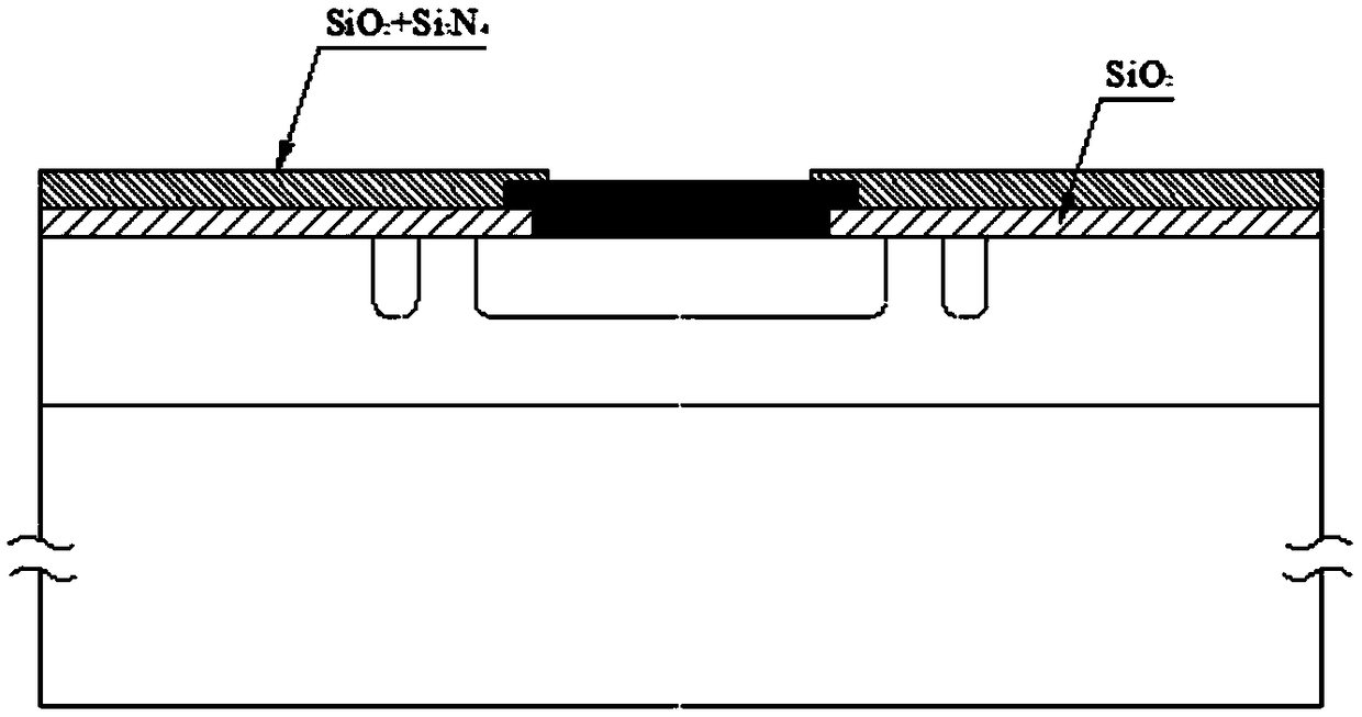
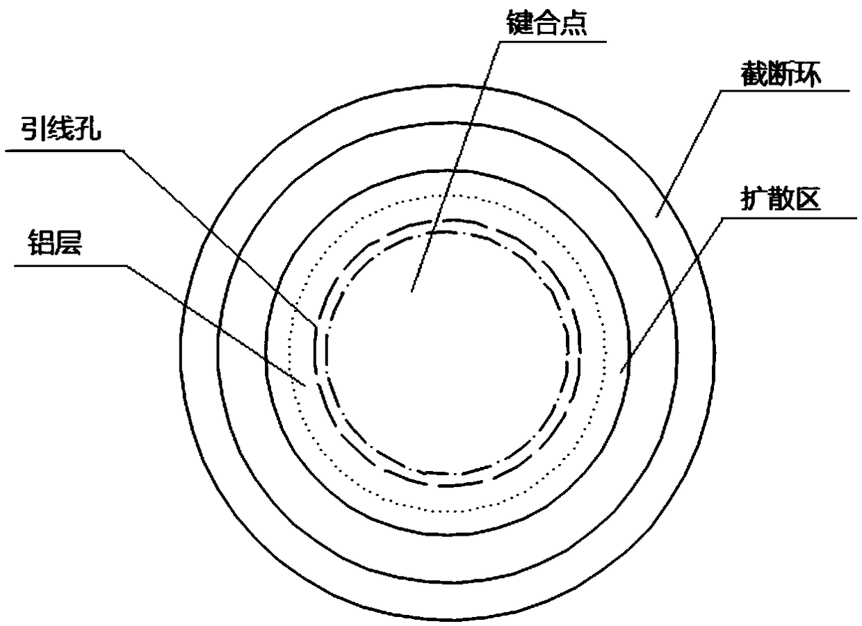
[0045] As introduced in the background technology, in the prior art, the capacitance of the diode barrier capacitance itself seriously affects the switching performance of the diode, resulting in long switching time and other shortcomings. In order to solve the above technical problems, this embodiment proposes a high-speed switching diode chip, such as figure 1 As shown, the cross-section of the chip is circular, including:
[0046] a substrate, an epitaxial layer is grown on the upper surface of the substrate;
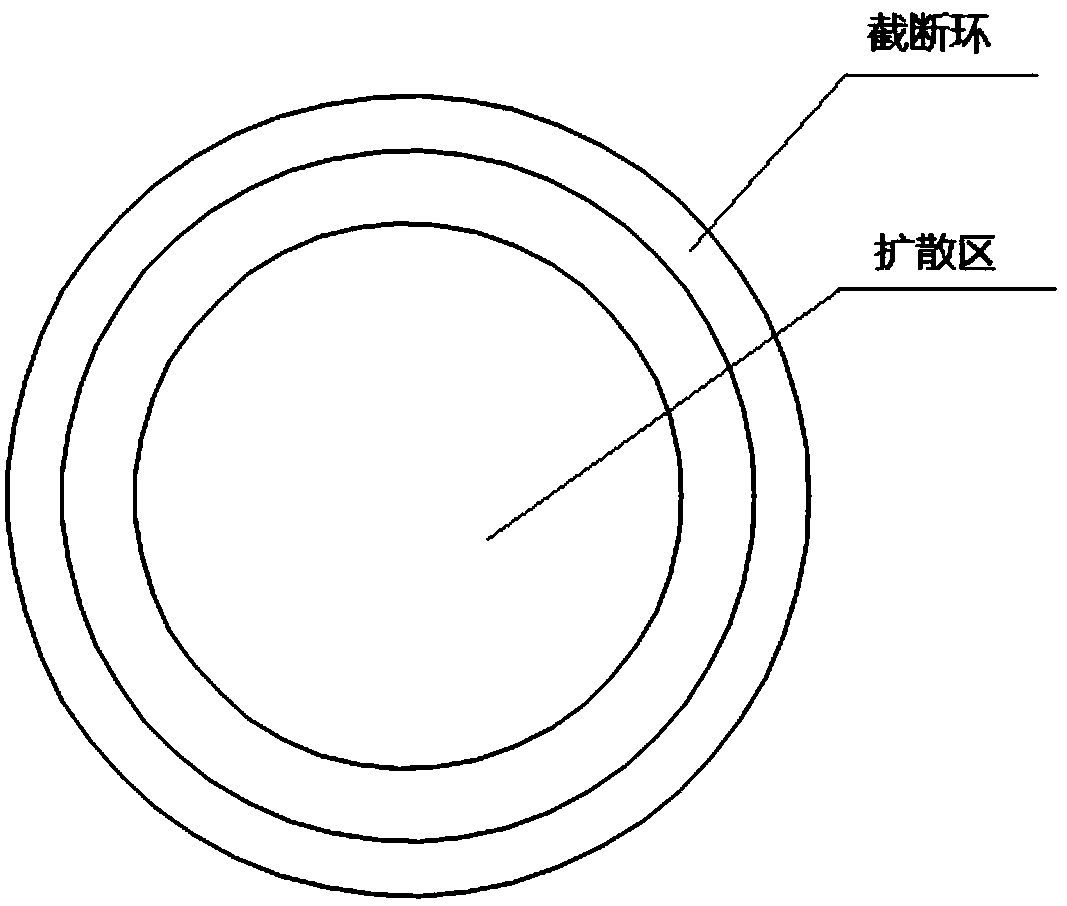
[0047] The upper surface of the epitaxial layer is a first oxide layer, and an annular isolation groove is photolithographically etched on the first oxide layer, the inside of the isolation groove is a diffusion area, and the outside of the isolation groove is a truncation ring;
[0048] The upper surface of the first oxide layer is a second oxide layer, and lead holes are photolithographically etched on the second oxide layer;
[0049] An evaporated aluminum layer...
Embodiment 2
[0064] The purpose of this embodiment is to provide the production process of the high-speed switching diode, including primary oxidation, photolithography in the diffusion area, diffusion in the diffusion area, secondary oxidation, photolithography of lead holes, steaming gold, gold diffusion, grinding, steaming aluminum, Aluminum anti-etching, alloying, and passivation, specifically, include the following steps:
[0065] (1) Once oxidized, a silicon dioxide film is generated on the surface of the epitaxial layer;
[0066] The process parameters are: temperature 1000℃~1200℃, oxygen flow 3.3~5.3L / min, hydrogen 3.3~5.3L / min, time 65~75min;
[0067] (2) Photolithography in the diffusion area, the area of the diffusion area is not greater than 1.33×10 5 μm 2 ;
[0068] The process parameters are: the speed of uniform glue is not less than 4000 rpm; the exposure time is not less than 35s.
[0069] (3) Diffusion in the diffusion area to obtain a diffusion area and a truncated...
PUM
Abstract
The invention discloses a high-speed switching diodechip and a production technology. The chip has a circular cross section and includes a substrate, wherein an upper surface of the substrate is provided with an epitaxial layer. An upper surface of the epitaxial layer is a first oxide layer, and an annular separation groove is formed on the first oxide layer through photoetching. A diffusion region is disposed in the separation groove, and a truncated ring is disposed outside the separation groove. A second oxide layer is formed on the upper surface of the first oxide layer, and a lead hole is formed on the second oxide layer through photoetching. A vaporized aluminum layer extends from the interior of the photoetched lead hole to the upper surface of the second oxide layer. The chip enables the switching time of a high-speed switching diode to be less than 5ns, the breakdown voltage to be greater than 100V, and the reverse leakage current to be less than 25nA.
Description
technical field [0001] The disclosure belongs to the technical field of diode chip manufacturing, and in particular relates to a high-speed switch diode chip and a production process. Background technique [0002] Switching diodes have the characteristics of fast switching speed, small size, long life, and high reliability. They are widely used in switching circuits, detection circuits, high-frequency and pulse rectification circuits and automatic control circuits of electronic equipment. For switching diodes, the most important characteristic is the behavior at high frequencies. [0003] At high frequencies, the barrier capacitance of the diode exhibits extremely low impedance and is connected in parallel with the diode. When the capacitance of the barrier capacitance itself reaches a certain level, it will seriously affect the switching performance of the diode. Therefore, the speed of switching the diode is the main indicator affecting the performance of the diode. [...
Claims
Application Information
Patent Timeline
Application Date:The date an application was filed.
Publication Date:The date a patent or application was officially published.
First Publication Date:The earliest publication date of a patent with the same application number.
Issue Date:Publication date of the patent grant document.
PCT Entry Date:The Entry date of PCT National Phase.
Estimated Expiry Date:The statutory expiry date of a patent right according to the Patent Law, and it is the longest term of protection that the patent right can achieve without the termination of the patent right due to other reasons(Term extension factor has been taken into account ).
Invalid Date:Actual expiry date is based on effective date or publication date of legal transaction data of invalid patent.

