Ultrahigh-frequency electromagnetic wave shielding film without chemical electroplating process and conductive particles, and manufacturing method of circuit board comprising film

A technology of ultra-high frequency electromagnetic waves and conductive particles, applied in chemical instruments and methods, magnetic field/electric field shielding, printed circuit components, etc., can solve the problems of relatively high size requirements of conductive particles, inability to pierce the shielding film, and affecting grounding, etc. , to achieve the effect of improving the overall shielding effect, saving production time, and improving barrier properties

Inactive Publication Date: 2019-03-01
深圳市西陆光电技术有限公司
View PDF5 Cites 6 Cited by
  • Summary
  • Abstract
  • Description
  • Claims
  • Application Information

AI Technical Summary

Problems solved by technology

Although this method can realize the free grounding of the shielding film and overcome the above technical difficulties, it has relatively high requirements on the size of conductive particles and high cost
Particles with special shapes and larger diameters are required to pierce the insulating covering film layer of the shielding film, and the particle size distribution of the conductive particles is required to be relatively uniform. If there are conductive particles with a particle size lower than the average particle size, there will be local failure to pierce the shielding film Insulating cover film, which in turn affects grounding

Method used


Image

  • Ultrahigh-frequency electromagnetic wave shielding film without chemical electroplating process and conductive particles, and manufacturing method of circuit board comprising film
  • Ultrahigh-frequency electromagnetic wave shielding film without chemical electroplating process and conductive particles, and manufacturing method of circuit board comprising film
  • Ultrahigh-frequency electromagnetic wave shielding film without chemical electroplating process and conductive particles, and manufacturing method of circuit board comprising film

Examples


Embodiment 1

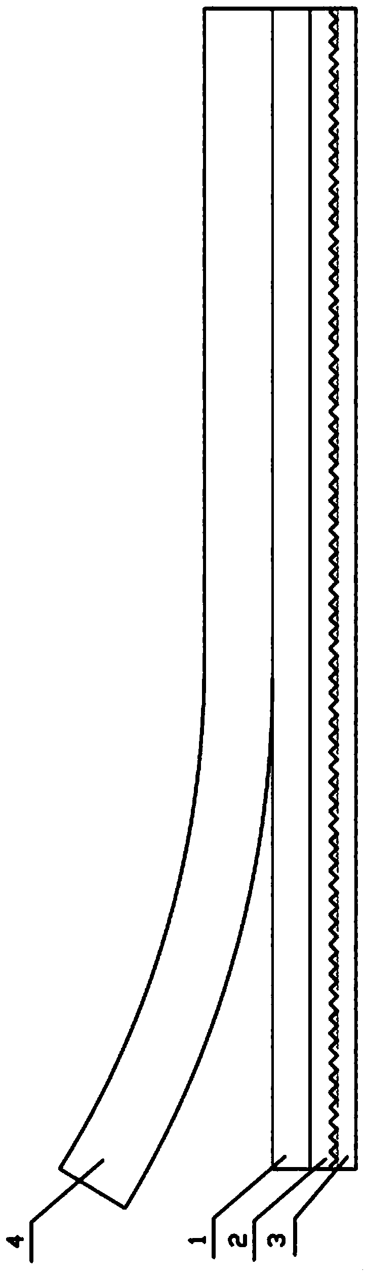
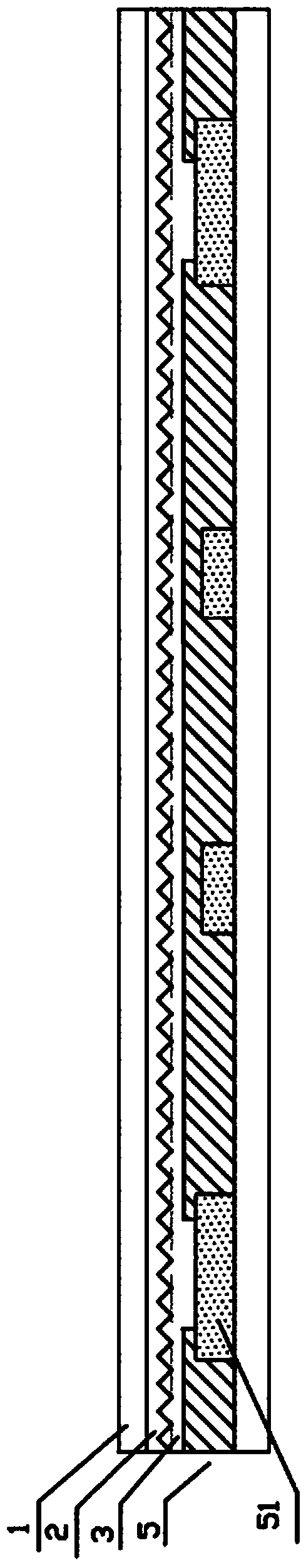
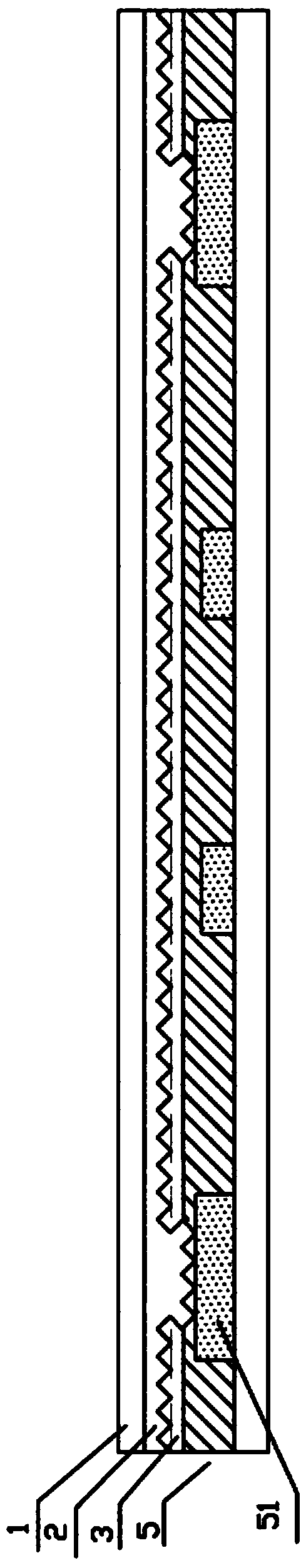
[0053] Such as figure 1 As shown, an electromagnetic wave shielding film for printed circuit boards, the carrier film 4 is provided with a special treatment roughened insulating layer 1, the specially treated roughened insulating layer 1 is provided with an alloy shielding layer 2, and the alloy shielding layer 2 is provided with a pure Adhesive film layer 3, wherein the carrier film is a PET release film, which can be peeled off from the specially treated roughened insulating layer 1.

[0054] The manufacturing method of the electromagnetic wave shielding film comprises the following steps:

[0055] 1) Form a specially treated roughened insulating layer on the carrier film 4: select a PET release film with a thickness of 25 to 150 microns and a width of 100 mm to 1000 mm, apply ink on the release surface side, and form after it is completely cured Roughen the insulation layer 1 by special treatment, the ink is epoxy resin ink or polyurethane ink, with a thickness of 1-25 mic...

Embodiment 2

[0061] Such as figure 1 As shown in the electromagnetic wave shielding film, the carrier film layer 4 is provided with a specially treated roughened insulating layer 1, the specially treated roughened insulating layer 1 is provided with an alloy shielding layer 2, and the alloy shielding layer 2 is provided with a pure rubber film layer 3. Wherein, the carrier film is a PET release film, which can be peeled off with the specially treated roughened insulating layer 1 .

[0062] The manufacturing method of the electromagnetic wave shielding film comprises the following steps:

[0063] 1) Form a specially treated roughened insulating layer on the carrier film layer 4: Select a PET release film with a thickness of 25-150 microns and a width of 100 mm to 1000 mm, and apply ink on the release surface side, and after it is completely cured Forming a specially treated roughened insulating layer 1, the ink is epoxy resin ink or polyurethane ink, with a thickness of 1-25 microns, prefe...


PUM

PropertyMeasurementUnit
thicknessaaaaaaaaaa
thicknessaaaaaaaaaa
thicknessaaaaaaaaaa

Abstract

The invention relates to the field of electromagnetic wave shielding films, in particular to an ultrahigh-frequency electromagnetic wave shielding film without a chemical electroplating process and conductive particles, and a manufacturing method of a circuit board comprising the film. The shielding film at least comprises an alloy shielding layer, wherein the outer surface of one side of the alloy shielding layer is coated with a pure adhesive layer; one or more of specially-processed coarsening insulation layers are arranged on the outer surface of the other side of an alloy shielding grounding layer; a carrier film layer is arranged on the outer surface of an insulating film layer; and the lower surface of a conductive adhesive layer is covered with a protection film. According to the shielding film, the pure adhesive film layer of the shielding film does not contain conductive particles, so that the cost can be lowered, and the insertion loss is reduced; and the pure adhesive filmlayer is punctured through the rough surface of the alloy shielding layer to realize grounding, so that extremely high shielding efficiency is achieved, the overall shielding effect is improved, pollution to the environment is reduced, the energy consumption is reduced, and the cost is lowered.

Description

technical field [0001] The invention relates to the technical field of electromagnetic wave shielding films, in particular to an ultra-high frequency electromagnetic wave shielding film without chemical plating process and conductive particles and a method for manufacturing a circuit board containing the film. Background technique [0002] Both flexible circuit boards and rigid-flexible circuit boards are printed circuit boards with high reliability and high flexibility made of polyimide or polyester film as the main flexible substrate. This kind of circuit board can be bent, folded, curled, and can be moved and stretched freely in three-dimensional space. The characteristics of flexible circuit boards can be used to reduce the size of electronic products, and realize the functions of light, thin, short or small products, so as to realize the integration of component devices and wire connections. Widely used in mobile phones, cameras, computers, communications or aerospace ...

Claims


Application Information

Patent Timeline
Patent Type & Authority Applications(China)
IPC IPC(8): H05K9/00H05K1/02B32B15/08B32B27/20B32B27/08B32B27/36B32B33/00C23C14/35C23C14/20
Inventor 林壁鹏
Owner 深圳市西陆光电技术有限公司
Why Eureka
Try Eureka