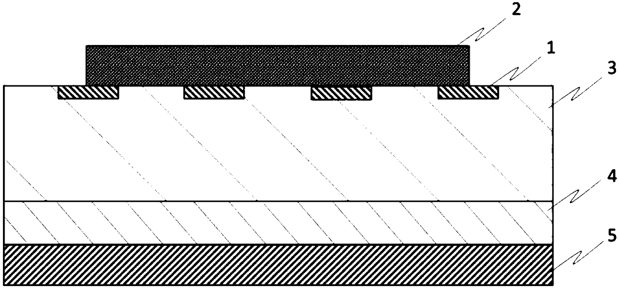
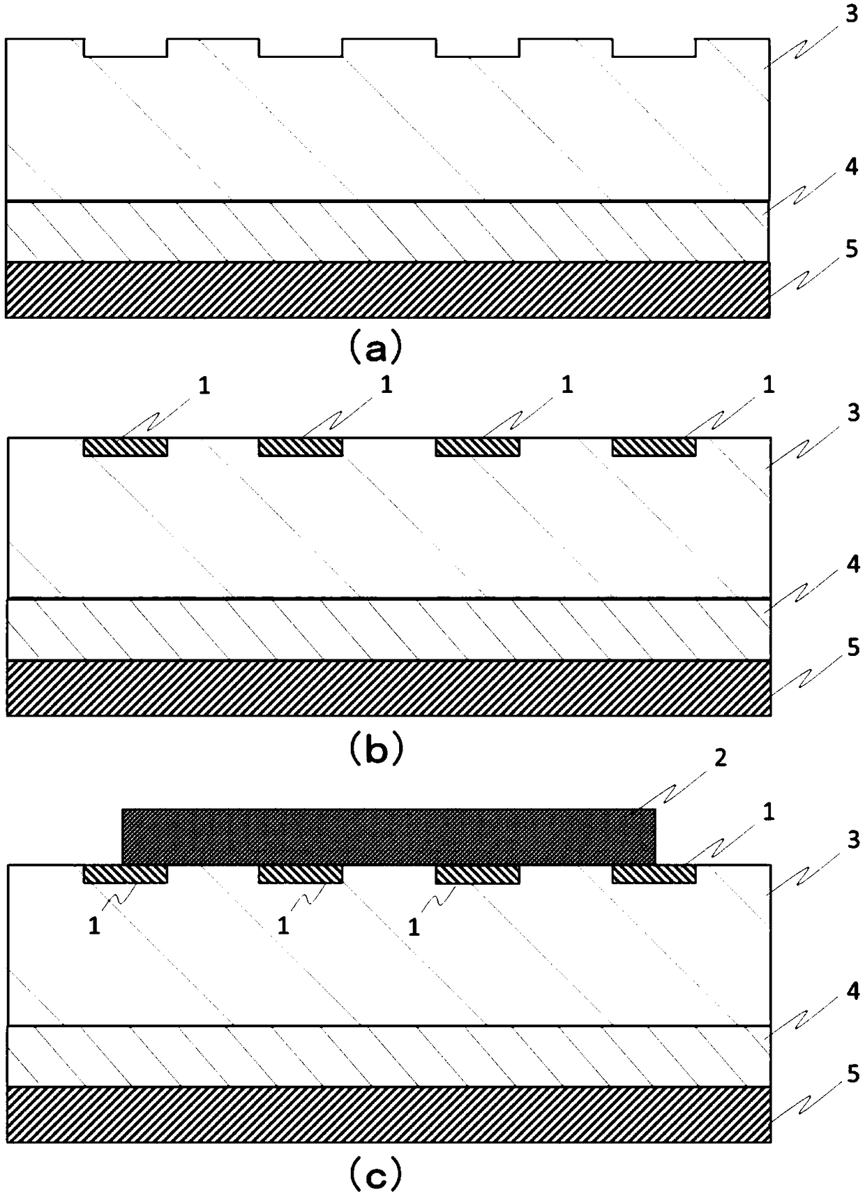
Semiconductor device

A semiconductor, n-type semiconductor technology, used in semiconductor devices, semiconductor/solid-state device manufacturing, electrical components, etc., can solve problems such as insufficient withstand voltage, reduced reverse recovery current, and insufficient PiN bonding

Pending Publication Date: 2019-03-05
FLOSFIA
View PDF5 Cites 4 Cited by
  • Summary
  • Abstract
  • Description
  • Claims
  • Application Information

AI Technical Summary

Problems solved by technology

However, due to the irradiation of protons, the interface between both the n-type semiconductor layer and the p-type semiconductor layer and the i-type semiconductor layer is adversely affected, and crystal defects are formed locally in the i-type semiconductor layer, resulting in The problem of reduced electrical characteristics of PiN diodes
In addition, electrical characteristics such as withstand voltage cannot be sufficiently satisfied.
[0004] In addition, Patent Document 2 describes that in order to increase the withstand voltage of a PiN diode, the i-type semiconductor layer is formed thicker to 50 μm or more, and the entire region of the i-type semiconductor layer contains oxygen to form atomic cavities bonded to oxygen. recombination defect, which reduces the reverse recovery current
However, the PiN diode described in Patent Document 2 needs to make the i-type semiconductor layer thicker than 50 μm in order to increase the withstand voltage, which has problems in miniaturization and cannot sufficiently satisfy the withstand voltage.
In addition, there is a problem that good PiN bonding cannot be achieved sufficiently

Method used


Image

  • Semiconductor device
  • Semiconductor device
  • Semiconductor device

Examples


Embodiment 1

[0087] (Example 1) Fabrication of a semiconductor device comprising an n-type semiconductor layer, an i-type semiconductor layer, and a p-type semiconductor layer

[0088] 1-1. Formation of n-type semiconductor layer

[0089] 1-1-1. Film forming device

[0090] use Figure 11, the spray CVD apparatus 19 used in the examples will be described. The spray CVD apparatus 19 includes: a susceptor 21 on which a substrate 20 is placed, a carrier gas supply unit 22a for supplying a carrier gas, a flow regulating valve 23a for adjusting the flow rate of the carrier gas sent from the carrier gas supply unit 22a, and a carrier gas supply unit 23a. (Dilution) carrier gas (dilution) supply unit 22b, flow regulating valve 23b for regulating the flow rate of the carrier gas sent from the carrier gas (dilution) supply unit 22b, accommodating the spray generation source 24 of raw material solution 24a, A container 25 into which water 25a can be placed, an ultrasonic vibrator 26 mounted on th...


PUM


Abstract

The invention provides a semiconductor device, which has excellent bonding among a p-type semiconductor layer, an n-type semiconductor layer and an i-type semiconductor layer, and has excellent semiconductor properties. According to the technical scheme, the semiconductor device is manufactured, and the obtained semiconductor device is used for a power device. The semiconductor device at least comprises the n-type semiconductor layer, the i-type semiconductor layer and the p-type semiconductor layer, wherein the n-type semiconductor layer comprises a first semiconductor as the main composition; the first semiconductor is an oxide semiconductor containing a metal selected from one or more than two of aluminum, indium, and gallium.

Description

technical field [0001] In particular, the present invention relates to semiconductor devices useful for power devices. Background technique [0002] PiN diodes having n-type semiconductor layers, i-type semiconductor layers and p-type semiconductor layers are known. When the PiN diode is turned on, holes are injected from the p-type semiconductor layer to the i-type semiconductor layer, electrons are injected from the n-type semiconductor layer to the i-type semiconductor layer, and conductivity modulation occurs in the i-type semiconductor layer. When the PiN diode is turned off, the carriers (holes and electrons) present in the high resistance region are discharged from the anode region and the cathode region, and the PiN diode becomes non-conductive. [0003] Patent Document 1 describes that in a PiN diode, protons are irradiated from both the n-type semiconductor layer side and the p-type semiconductor layer side toward the i-type semiconductor layer side, and the inter...

Claims


Application Information

Patent Timeline
IPC IPC(8): H01L29/04H01L29/24H01L29/868H01L29/872
CPCH01L29/04H01L29/24H01L29/868H01L29/872H01L29/66969H01L29/045H01L21/02483H01L21/02502H01L21/02565H01L21/02576H01L21/02579H01L21/02581H01L21/0262H01L21/02628H01L29/0619H01L29/063
Inventor 杉本雅裕髙桥勲四户孝人罗俊实
Owner FLOSFIA
Why Eureka
Try Eureka