Electroluminescent compound, OLED display panel and electronic equipment

A display panel and luminescence technology, which is applied to compounds of elements of group 5/15 of the periodic table, compounds containing elements of group 3/13 of the periodic table, luminescent materials, etc., can solve problems such as performance needs to be improved, and achieve improved The effect of luminous efficiency

Inactive Publication Date: 2019-03-08
WUHAN TIANMA MICRO ELECTRONICS CO LTD
View PDF4 Cites 16 Cited by
  • Summary
  • Abstract
  • Description
  • Claims
  • Application Information

AI Technical Summary

Problems solved by technology

However, there are few TADF materials that have been discovered so far, and the performance nee...

Method used


Image

  • Electroluminescent compound, OLED display panel and electronic equipment
  • Electroluminescent compound, OLED display panel and electronic equipment
  • Electroluminescent compound, OLED display panel and electronic equipment

Examples


preparation example Construction

[0066] The preparation method of the compound provided by the present invention is prior art, and the synthetic method of following compound is provided exemplarily below:

[0067] (1)A 1 and A 2 When each is independently selected from a group containing a carbonyl group, the synthesis method is as follows (taking M3 as an example):

[0068]

[0069] Weigh S1(30mmol), S2(65mmol), Pd(OAc) 2 (1.5mmol), P(t-Bu) 3 (3mmol) and K 2 CO 3 (120mmol), add 120mL toluene to dissolve. Under nitrogen atmosphere, it was heated to 120° C. for 48 h. The reaction mixture was cooled to room temperature. The reaction mixture was poured into 600 mL of cold water and stirred for 6 h. Extract with dichloromethane (3 x 60 mL) and collect the organic phase. with anhydrous Na 2 SO 4 The organic phase is dried. The solvent was distilled off under reduced pressure to obtain a crude product. Finally, the sample was purified by column chromatography to obtain the target product M3 (23.4 mm...

Embodiment 1

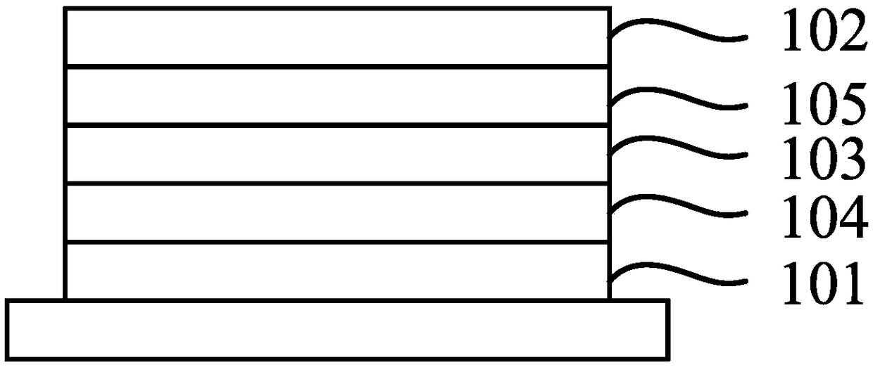
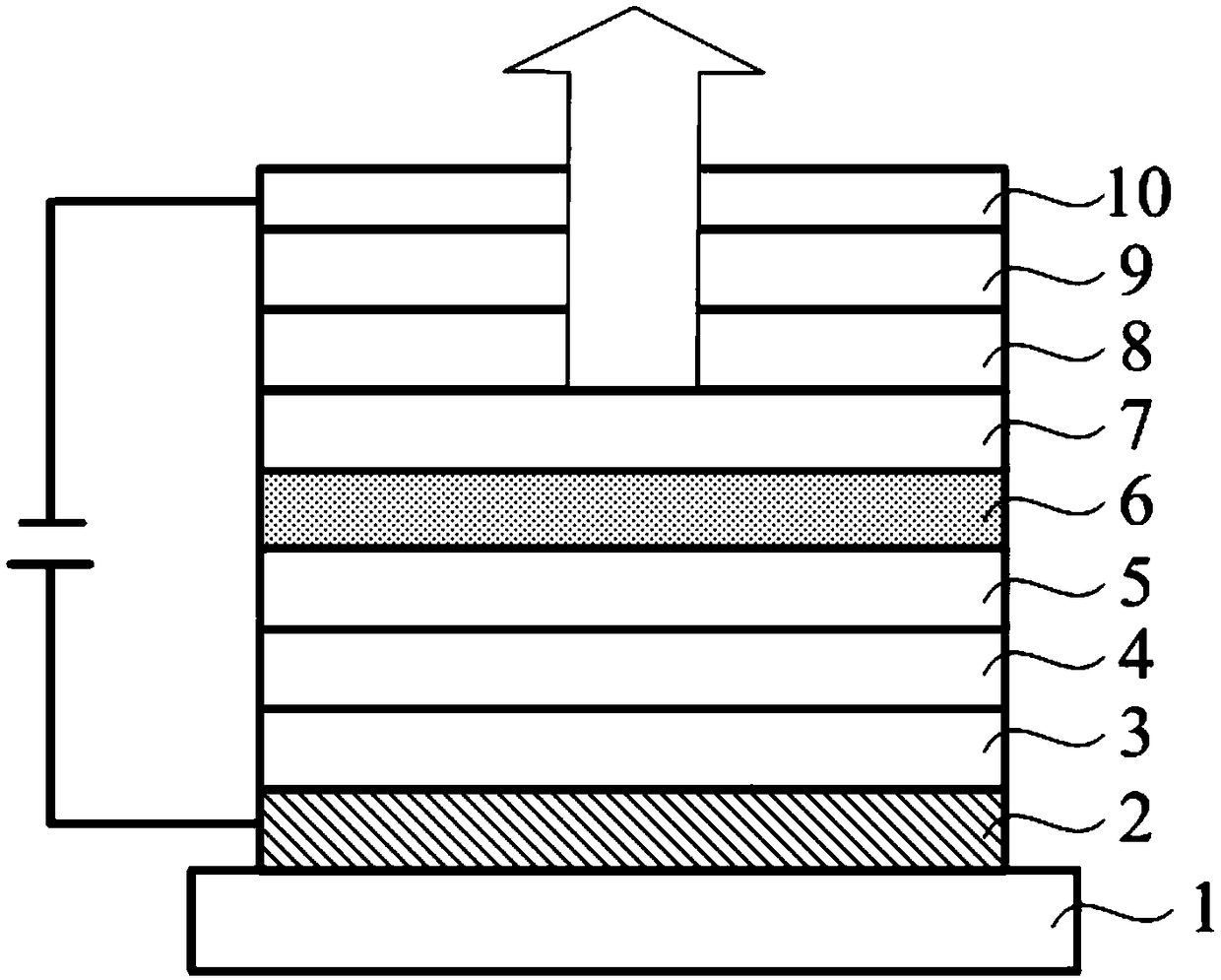
[0081] This embodiment provides an OLED display panel N1, such as figure 2 As shown, the display panel includes: a substrate 1, an ITO anode 2, a hole injection layer 3, a first hole transport layer 4, a second hole transport layer 5, a light emitting layer 6, a first electron transport layer 7, a second electron transport layer Transport layer 8, electron injection layer 9 and cathode 10 (aluminum electrode), wherein the thickness of ITO anode 2 is 10nm, the thickness of hole injection layer 3 is 5nm, the thickness of the first hole transport layer 4 is 50nm, the second hole The thickness of the hole transport layer 5 is 10nm, the thickness of the light emitting layer 6 is 20nm, the thickness of the first electron transport layer 7 is 5nm, the thickness of the second electron transport layer 8 is 20nm, the thickness of the electron injection layer 9 is 1nm, the aluminum electrode The thickness of 10 is 15 nm.

[0082] The preparation steps of the OLED display panel N1 are a...

Embodiment 2

[0095] The difference from Example 1 is that an OLED display panel N2 is provided, and compound M1 is replaced by compound M2


PUM

PropertyMeasurementUnit
Thicknessaaaaaaaaaa
Thicknessaaaaaaaaaa
Thicknessaaaaaaaaaa

Abstract

The invention provides an electroluminescent compound, an OLED display panel and electronic equipment. The electroluminescent compound is provided with a structure of a formula (I); the OLED display panel comprises an anode, a cathode and at least one organic film layer positioned between the anode and the cathode, and the organic film layer comprises a luminescent layer; the luminescent layer comprises any one or a combination of at least two of the electroluminescent compounds; and the electronic equipment comprises the OLED display panel. The electroluminescent compound provided by the invention has an energy electrode difference Delta Est between the lowest singlet state S1 and the lowest triplet state T1, wherein the Delta Estwhich is equal to ES1 minus ET1 being less than or equal to0.30 eV, and even the Delta Est which is equal to ES1 minus ET1 being less than or equal to 0.15 eV; and the electroluminescent compound has an TADF (Thermal Activation Delayed Fluorescence) materiallight-emitting mechanism, can be used in the field of organic photoelectric devices, and improves light-emitting efficiency, so thatthe electronic equipment comprising the electroluminescent compoundhas more excellent performance.

Description

technical field [0001] The invention relates to the technical field of organic electroluminescent materials, in particular to an electroluminescent compound, an OLED display panel and electronic equipment. Background technique [0002] Organic light-emitting materials can be roughly divided into four categories according to the light-emitting mechanism: traditional fluorescent materials, phosphorescent materials, triplet-triplet annihilation (TTA) materials, and thermally activated delayed fluorescence (TADF) materials. Among them, the highest internal quantum efficiency of traditional fluorescent materials is only 25%, and the theoretical maximum internal quantum yield of TTA materials does not exceed 62.5%. Although the theoretical maximum internal quantum yield of phosphorescent materials can reach 100%, they usually contain rare and precious metals, resulting in high prices. Expensive, poor device stability, serious device efficiency decline and other issues have further...

Claims


Application Information

Patent Timeline
IPC IPC(8): C07D471/10C07D519/00C07F5/02C07F9/36C07F9/6571C07F9/6561C09K11/06H01L51/50H01L51/54
CPCC09K11/06C07D471/10C07D519/00C07F5/025C07F5/027C07F9/36C07F9/6561C07F9/65615C07F9/657127C09K2211/1011C09K2211/1029C09K2211/1007C09K2211/1092C09K2211/1096H10K85/615H10K85/626H10K85/6576H10K85/657H10K85/6572H10K50/11
Inventor 高威张磊朱晴牛晶华安平
Owner WUHAN TIANMA MICRO ELECTRONICS CO LTD
Why Eureka
Try Eureka