High mobility light emitting semiconductor and preparation method, use and application method thereof

A light-emitting semiconductor, high-mobility technology, used in semiconductor/solid-state device manufacturing, semiconductor devices, luminescent materials, etc., to achieve the effect of high luminous efficiency and high electron mobility

Active Publication Date: 2019-03-12
THE HONG KONG UNIV OF SCI & TECH
View PDF2 Cites 3 Cited by
  • Summary
  • Abstract
  • Description
  • Claims
  • Application Information

AI Technical Summary

Problems solved by technology

Although high-mobility organic semiconductors and high-efficiency organic light-emitting diodes have been well developed, organic semiconductor materials with high mobility and high luminance are still a challenge.

Method used


Image

  • High mobility light emitting semiconductor and preparation method, use and application method thereof
  • High mobility light emitting semiconductor and preparation method, use and application method thereof
  • High mobility light emitting semiconductor and preparation method, use and application method thereof

Examples


Embodiment Construction

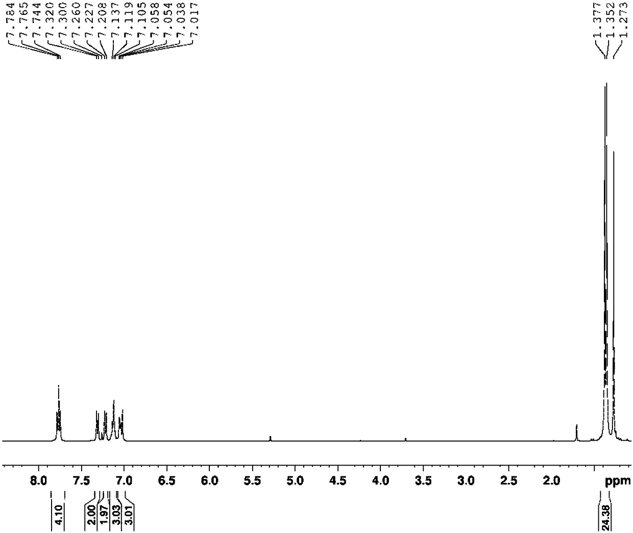
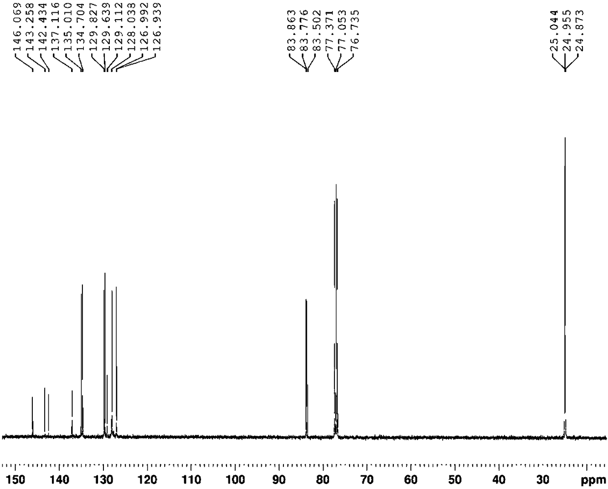
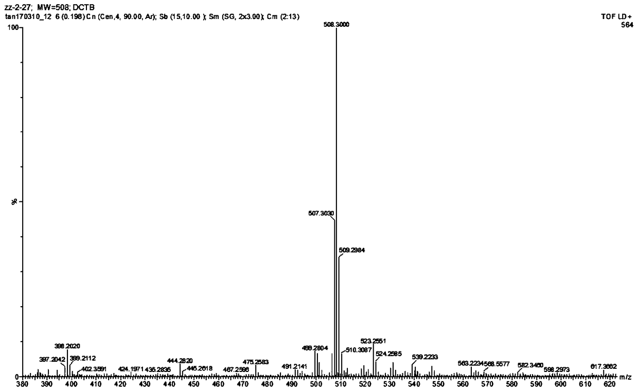
[0057] In order to have a clearer understanding of the technical features, purposes and effects of the present invention, the specific implementation manners of the present invention will now be described in detail with reference to the accompanying drawings. Apparently, the described embodiments are only some of the embodiments of the present invention, but not all of them. Based on the embodiments of the present invention, all other embodiments obtained by persons of ordinary skill in the art without making creative efforts belong to the protection scope of the present invention.

[0058] The high-mobility aggregation-induced luminescent material is characterized in that it includes the following chemical formula:

[0059]

[0060] R1, R2 and R3 are H or various imide receptors, wherein the receptors specifically include the following structural formula:

[0061]

[0062] R5 is an alkyl chain or glycol chain C n o m h 2n+1O , n=1~24 and m=0~10, the number of C in R...


PUM


Abstract

The invention discloses a high mobility light emitting semiconductor and a preparation method thereof, use and application method thereof. The preparation method of a high mobility light emitting semiconductor comprises a Suzuki coupling chemical reaction between an aryl bromide or an iodide and an aryl boronic acid or a boric acid ester. In the application method of the high mobility light emitting semiconductor to a device, the device uses a bottom gate top contact device structure, the gate uses n-type doped silicon, and a 300 nm SiO2 is thermally grown as an insulating layer, before depositing the organic semiconductor layer, the gate insulating layer is modified by OTS in a vacuum furnace at 120 DEG C to form a single-layer OTS modified layer; the modified layer is successively washedwith chloroform, n-hexane, isopropanol and acetone, and the high mobility light-emitting semiconductor is utilized for film coating in a manner of spin coating. The material synthesized by the invention exhibits the property of aggregation-induced luminescence, and the conventional fluorescent dye has the phenomenon of aggregation-induced fluorescence quenching under high concentration conditions. Therefore, the invention effectively overcomes the defects of the conventional fluorescent dye.

Description

technical field [0001] The invention belongs to the technical field of organic photoelectric materials, and in particular relates to a high-mobility light-emitting semiconductor and its preparation method, use and application method. Background technique [0002] Organic semiconductors have important applications in many flexible optoelectronic devices such as organic light-emitting diodes, organic field-effect transistors, and organic photovoltaics. Although both high-mobility organic semiconductors and high-efficiency organic light-emitting diodes have been well developed, organic semiconductor materials with high mobility and high luminance are still a challenge. High-mobility organic light-emitting semiconductors can be used to prepare postal light-emitting transistors, pump lasers, etc. In addition, near-infrared organic light-emitting semiconductors have applications in night vision, encrypted displays, and fluorescent probes. Contents of the invention [0003] The ...

Claims


Application Information

Patent Timeline
Patent Type & Authority Applications(China)
IPC IPC(8): C07D471/06C09K11/06H01L51/00H01L51/54H10K99/00
CPCC09K11/06C07D471/06C09K2211/1029C09K2211/1007H10K85/60H10K85/6572
Inventor 唐本忠赵征
Owner THE HONG KONG UNIV OF SCI & TECH
Why Eureka
Try Eureka