

Coaxial TSV-structure pinboard and fabrication method thereof
A manufacturing method and a technology of an adapter board, applied in semiconductor/solid-state device manufacturing, electrical components, electrical solid-state devices, etc., can solve the complex manufacturing process of coaxial TSV structures, the selection of intermediate dielectric layer materials, and the repeatability of manufacturing methods and processes Difficult, unable to achieve engineering mass production and other issues, to achieve ultra-vertical transmission loss, controllable repeatability, and low cost effects
- Summary
- Abstract
- Description
- Claims
- Application Information
AI Technical Summary
Problems solved by technology
Method used
Image

Examples
Embodiment 1
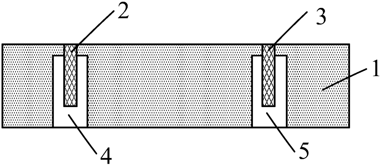
[0040] The coaxial TSV structure adapter plate of the present invention includes an outer ring metal layer, an intermediate dielectric layer and an inner ring copper column structure; wherein the thickness of the outer ring metal layer is between 1-2 μm to achieve side wall metallization , the diameter of the inner ring copper pillar structure is between 20-30 μm, the thickness of the intermediate dielectric layer is adjustable to achieve 50 ohm matching with the outer ring metal layer and the inner ring copper pillar structure, the middle The thickness range of the dielectric layer is generally between 10-20 μm, and the depth of the coaxial TSV structure is 200 μm.
[0041] In order to manufacture the adapter plate, the present invention provides a method for manufacturing an adapter plate with a coaxial TSV structure, which at least includes the following steps:
[0042] Step S1: preprocessing the silicon wafer, the silicon wafer has a corresponding front side and a back sid...
Embodiment 2
[0066] In this embodiment, the thickness of the metal layer of the outer ring is 1.5 μm, the diameter of the copper pillar structure of the inner ring is 20 μm, and the intermediate dielectric layer is selected from benzocyclobutene (BCB, dielectric constant 2.65, dielectric loss 0.0008) The thickness is 20 μm to achieve 50 ohm matching between the intermediate dielectric layer and the outer ring metal layer and the inner ring copper pillar structure, and the depth of the coaxial TSV structure is 200 μm. Such as Figures 1 to 8 As shown, in order to manufacture the coaxial TSV structure adapter plate of this embodiment, the present invention provides a method for manufacturing a coaxial TSV structure adapter plate, which at least includes the following steps:
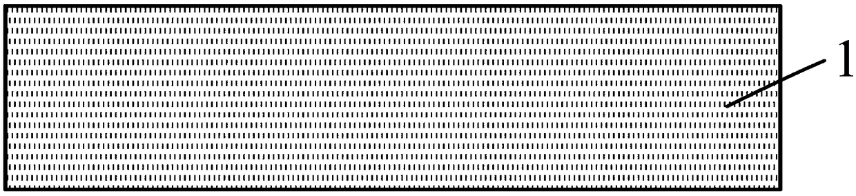
[0067] Step S1: Provide a silicon wafer 1, crystal orientation, polished on both sides, with a thickness of 320 μm, see figure 1 ;
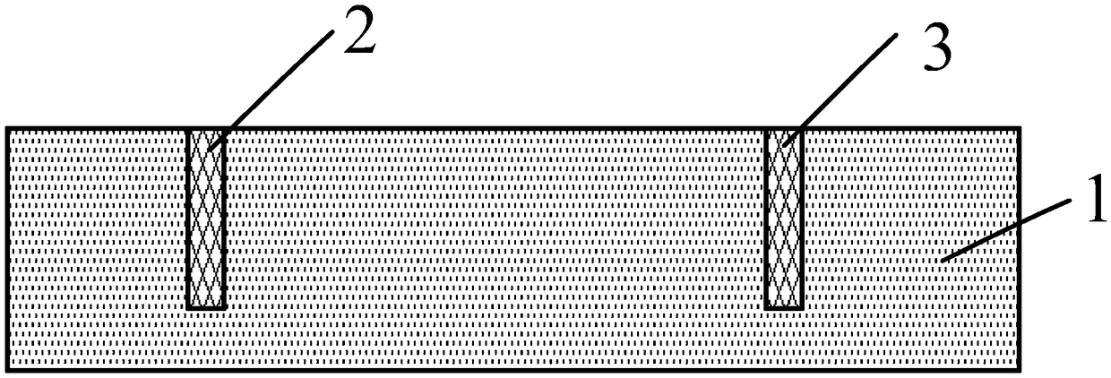
[0068] Step S2 : on the front side of the silicon wafer 1 , fabricate a first inner...
Embodiment 3
[0084] In the coaxial TSV structure adapter plate of this embodiment, the thickness of the outer ring metal layer is 1.5 μm, the diameter of the metal copper column is 30 μm, and the intermediate dielectric layer is polyimide (PI, dielectric The constant is 2.9, the dielectric loss is 0.01) and the thickness is 47.5 μm, which can realize 50 ohm matching with the outer ring metal layer and the inner ring copper pillar structure, and the depth of the coaxial TSV structure is 200 μm.
[0085] In this embodiment, the manufacturing method of the coaxial TSV structure adapter plate at least includes the following steps:
[0086] Step S1: Provide a silicon wafer 1 with a crystal orientation, double-sided polishing, and a thickness of 320 μm;
[0087] Step S2 : on the front side of the silicon wafer 1 , fabricate the first inner copper pillar structure 2 and the second inner copper pillar structure 3 . First, AZ4620 photoresist is spin-coated on the front side of the silicon wafer 1...
PUM
| Property | Measurement | Unit |
|---|---|---|
| Thickness | aaaaa | aaaaa |
| Thickness | aaaaa | aaaaa |
| Thickness | aaaaa | aaaaa |
Abstract
Description
Claims
Application Information