Universal manufacturing device for integrated circuits

A technology for manufacturing devices and integrated circuits, applied in the field of general-purpose manufacturing devices for integrated circuits, can solve the problems of increasing labor intensity of manual cleaning, reducing wafer processing efficiency, and wafer surface collision damage, saving labor intensity and having a wide range of applications. , the effect of increasing the usable area

Active Publication Date: 2019-03-22
广东嗨学云教育科技有限公司
View PDF25 Cites 2 Cited by
  • Summary
  • Abstract
  • Description
  • Claims
  • Application Information

AI Technical Summary

Problems solved by technology

[0003] The present invention provides a general-purpose manufacturing device for integrated circuits, which can effectively solve the traditional dust-collecting circuit wafer manufacturing proposed in the above-mentioned background technology due to the lack of a complete set of slicing, polishing, cleaning and other manufacturing devices, resulting in long time for wafer manufacturing. Relatively long and low yield rate of finished products, and the traditional slicing and polishing manufacturing equipment lacks waste collection components, resulting in the waste and debris generated after cutting and grinding cannot be cleaned in the first place, not only easy It will pollute the inside of the manufacturing device and increase the labor intensity of manual cleaning. At the same time, the existing manufacturing device lacks stirring and mixing components during the cleaning process or generally uses solids to stir the wafer. The former makes the wafer The cleaning effect is poor, and the latter is likely to cause collision damage to the surface of the wafer. In addition, the existing manufacturing equipment generally dries the wafer by draining and drying, which leads to a long drying time and reduces the wafer surface. The problem of round processing efficiency

Method used


Image

  • Universal manufacturing device for integrated circuits
  • Universal manufacturing device for integrated circuits
  • Universal manufacturing device for integrated circuits

Examples


Embodiment

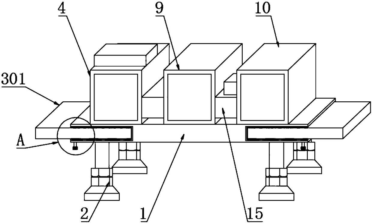
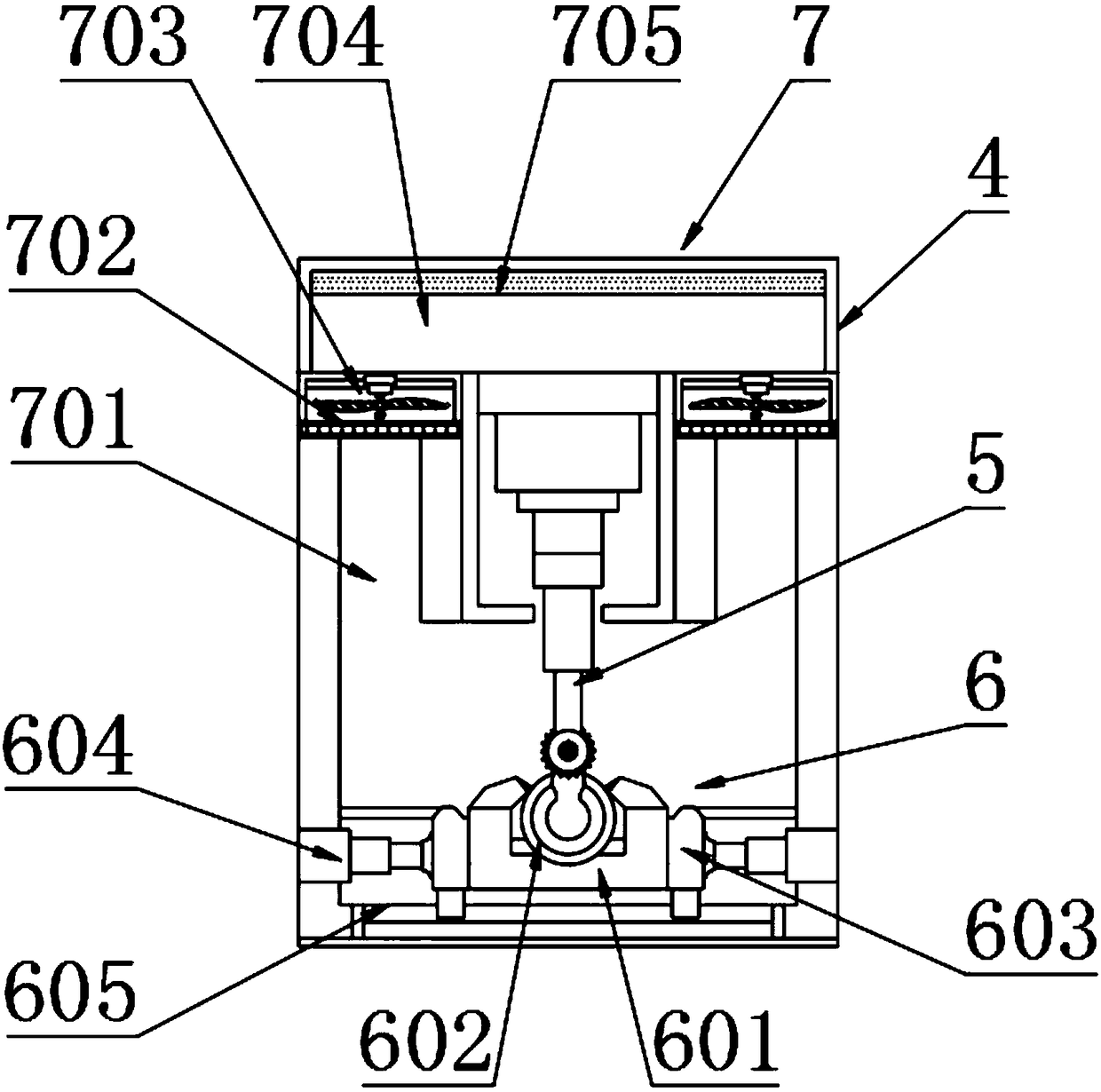
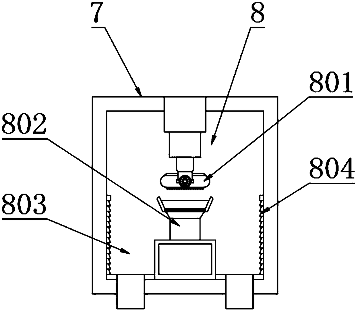
[0030] Example: such as Figure 1-6As shown, the present invention provides a technical solution, a general integrated circuit manufacturing device, including a manufacturing table 1, and an adjustable support 2 is fixedly supported by welding under the bottom of the manufacturing table 1, in order to facilitate the adjustment of the overall height of the manufacturing table 1 , and at the same time make the adjustable support 2 more stable when supporting the manufacturing table 1, the bottom of the adjustable support 2 is provided with an adjusting bolt, and the bottom of the adjustable support 2 is provided with anti-slip gaskets, and the two sides of the manufacturing table 1 Stretching components 3 are symmetrically installed on all parts. The stretching components 3 include a stretching table 301, a fitting chute 302, a movable roller 303 and a fastening knob 304. The inner side of the manufacturing table 1 is provided with a fitting chute 302. The middle part of the inn...


PUM


Abstract

The invention discloses a universal manufacturing device for integrated circuits. The universal manufacturing device for the integrated circuits comprises a manufacturing table. An abrasion cutting machine box is fixedly installed above the edge portion of one side of the manufacturing table. A slicing machine is fixedly installed in one edge portion of the inner side of the abrasion cutting machine box. A clamping assembly is arranged below the bottom of the slicing machine. According to the universal manufacturing device for the integrated circuits, the structure is scientific and reasonable; and the use is safe and convenient. A dust suction fan is arranged so that the excess material excised by the slicing machine can be sucked in time into a dirt collecting cavity and collected; the cleaning effect is good; and labor intensity of manual cleaning is lowered. Fragments ground by a polishing machine are collected conveniently through fragment grooves and stream guidance racks, and pollution to the interior of the abrasion cutting machine box caused by overflowing of the fragments is prevented. A silicon rod is conveniently fixed and clamped through a clamping table and a fastening ring, then deviating movement is not generated when the silicon rod is sliced, and then accuracy of slicing is guaranteed. Silicon rods of different diameters are conveniently adjusted and clamped by the device through movable regulation of limiting pushing blocks, hydraulic push rods and a sliding base. The application range is wide.

Description

technical field [0001] The invention relates to the technical field of integrated circuits, in particular to a general manufacturing device for integrated circuits. Background technique [0002] With the continuous development of the current society, the scope of use of integrated circuits is also increasing. Integrated circuits are microelectronic devices or components that use a certain process to combine transistors, resistors, capacitors and Components such as inductors and wiring are interconnected together, fabricated on a small or several small semiconductor wafers or dielectric substrates, and then packaged in a package to become a microstructure with the required circuit functions; all components have been structurally Formed as a whole, the electronic components have taken a big step towards miniaturization, low power consumption, intelligence and high reliability. The integrated circuit is a new type of semiconductor device, which is processed by oxidation, photol...

Claims


Application Information

Patent Timeline
Patent Type & Authority Applications(China)
IPC IPC(8): B08B3/10B08B3/14B24B9/06B24B41/06B24B55/06B25H1/14B28D5/00B28D5/02H05B3/00
CPCH05B3/00B08B3/102B08B3/14B24B9/065B24B41/068B24B55/06B25H1/14B28D5/0076B28D5/0082B28D5/022
Inventor 王强
Owner 广东嗨学云教育科技有限公司
Why Eureka
Try Eureka