Method and single crystal furnace for preparing n-type single crystal silicon

A single crystal silicon, n-type technology, applied in the field of preparing n-type single crystal silicon, can solve the problems of increasing the usable length, changing the crystal resistivity, and short usable length of lightly doped n-type single crystal silicon, etc.

Active Publication Date: 2021-02-05
XUZHOU XINJING SEMICON TECH CO LTD +1
View PDF7 Cites 0 Cited by
  • Summary
  • Abstract
  • Description
  • Claims
  • Application Information

AI Technical Summary

Problems solved by technology

For this reason, an object of the present invention is to propose a method for preparing n-type single crystal silicon, which can effectively change the crystal resistivity, increase the available length of compliance, and then effectively solve the problem of light doping with a resistivity greater than 50ohm·cm. The available length of n-type monocrystalline silicon is too short and the yield is too poor

Method used


Image

  • Method and single crystal furnace for preparing n-type single crystal silicon
  • Method and single crystal furnace for preparing n-type single crystal silicon
  • Method and single crystal furnace for preparing n-type single crystal silicon

Examples


Embodiment 1

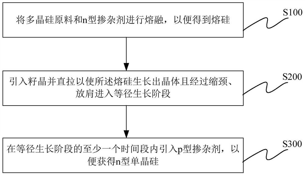
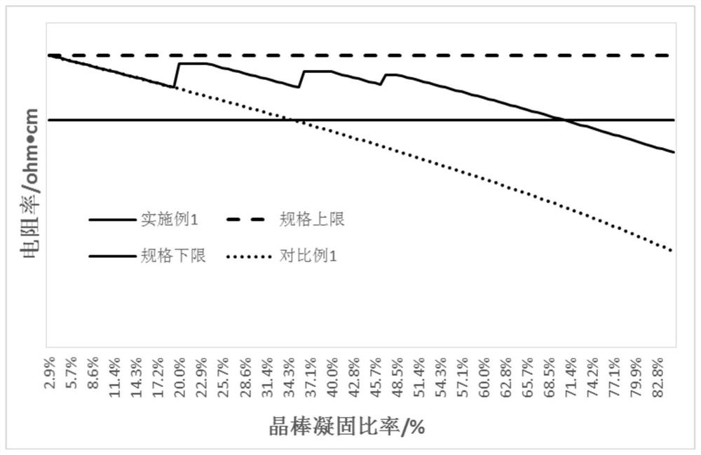
[0066] (1) Melt polysilicon raw material and n-type dopant to obtain molten silicon. The mass of polysilicon raw material is 250kg, and the doping amount of n-type dopant is 0.62g, according to the normal chemical process.

[0067] (2) introducing a seed crystal and pulling it straight so that the molten silicon grows into a crystal and goes through the stages of necking, shouldering, and equal diameter growth;

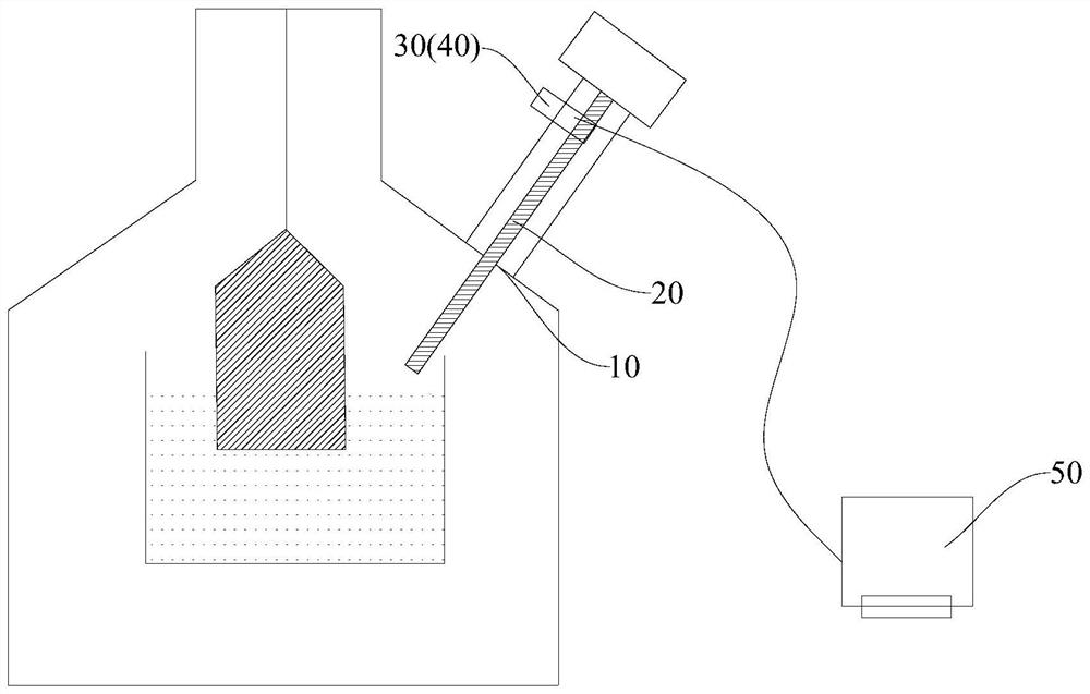
[0068] (3) Diborane is passed into the single crystal furnace in the 6th hour, the 12th hour, and the 20th hour when the equal-diameter growth stage begins. The concentration of diborane is 500ppm, and the gas flow rate of feeding diborane is 300sccm , the access time is 1 minute.

[0069] (4) Obtain n-type single crystal silicon.

Embodiment 2

[0071] (1) Melt the polysilicon raw material and n-type dopant to obtain molten silicon. The mass of polysilicon raw material is 250kg, and the doping amount of n-type dopant is 0.67g, according to the normal chemical process.

[0072] (2) introducing a seed crystal and pulling it straight so that the molten silicon grows into a crystal and goes through the stages of necking, shouldering, and equal diameter growth;

[0073] (3) in the 3rd hour, the 9th hour, the 15th hour, the 23rd hour in the equidiametrical growth stage, pass into diborane in the single crystal furnace, the concentration of diborane is 300ppm, pass into diborane The gas flow rate is 100 sccm, and the passing time is 0.5-1 minute.

[0074] (4) Obtain n-type single crystal silicon.


PUM


Abstract

The invention discloses a method for preparing n-type single crystal silicon and a single crystal furnace, wherein the method for preparing the n-type single crystal silicon comprises the following steps: melting a polycrystalline silicon raw material and an n-type dopant to obtain molten silicon; introducing a seed crystal and straightening to enable crystals to grow out of the molten silicon, and subjecting the crystals to necking and shouldering so as to enter an equal diameter growth stage; and introducing a p-type dopant in at least one period of the equal diameter growth stage to obtainthe n-type single crystal silicon. By adopting the method, the crystal resistivity can be effectively changed, and the usable length can be increased for compliance, so that the problems that the light-doped n-type single crystal silicon having the resistivity greater than 50 ohm.cm is too short in usable length and too poor in yield can be effectively solved.

Description

technical field [0001] The invention relates to the field of single crystal silicon, in particular, the invention relates to a method and a single crystal furnace for preparing n-type single crystal silicon. Background technique [0002] The dopant present in the molten soup will precipitate from the solid-liquid interface into the solid phase (that is, the ingot) during the crystal growth process. Since the solubility of impurities in the solid phase may be different from that in the liquid phase, the concentration of the dopant precipitated out of the solid phase is not equal to the concentration in the liquid phase. This phase is called segregation. The ratio of solid impurity concentration to liquid impurity concentration is called the segregation coefficient. [0003] Generally, the dopant of lightly doped n-type single crystal silicon is phosphorus, and the segregation coefficient of phosphorus is 0.35. The resistivity range of the equal diameter length of the drawn w...

Claims


Application Information

Patent Timeline
Patent Type & Authority Patents(China)
IPC IPC(8): C30B15/04C30B29/06
CPCC30B15/04C30B29/06
Inventor 郑加镇
Owner XUZHOU XINJING SEMICON TECH CO LTD
Why Eureka
Try Eureka