Millimeter wave amplifier chip testing cavity and method

A technology of chip testing and millimeter wave, which is applied in the direction of electronic circuit testing, instruments, measuring electronics, etc., can solve the problems that cannot meet the requirements of high-frequency millimeter wave amplifier chip testing, the module realizes the use of millimeter wave front-end systems, and high operating frequency, so as to reduce the The effect of small loss and simple design structure

Active Publication Date: 2019-03-22
HANGZHOU DIANZI UNIV +1
View PDF6 Cites 0 Cited by
  • Summary
  • Abstract
  • Description
  • Claims
  • Application Information

AI Technical Summary

Problems solved by technology

However, the millimeter-wave amplifier chip test device in the form of a coaxial interface can only work at a frequency up to 145GHz (0.8mm interface), wh

Method used


Image

  • Millimeter wave amplifier chip testing cavity and method
  • Millimeter wave amplifier chip testing cavity and method
  • Millimeter wave amplifier chip testing cavity and method

Examples


Embodiment Construction

[0024] The present invention will be further described below in conjunction with accompanying drawing.

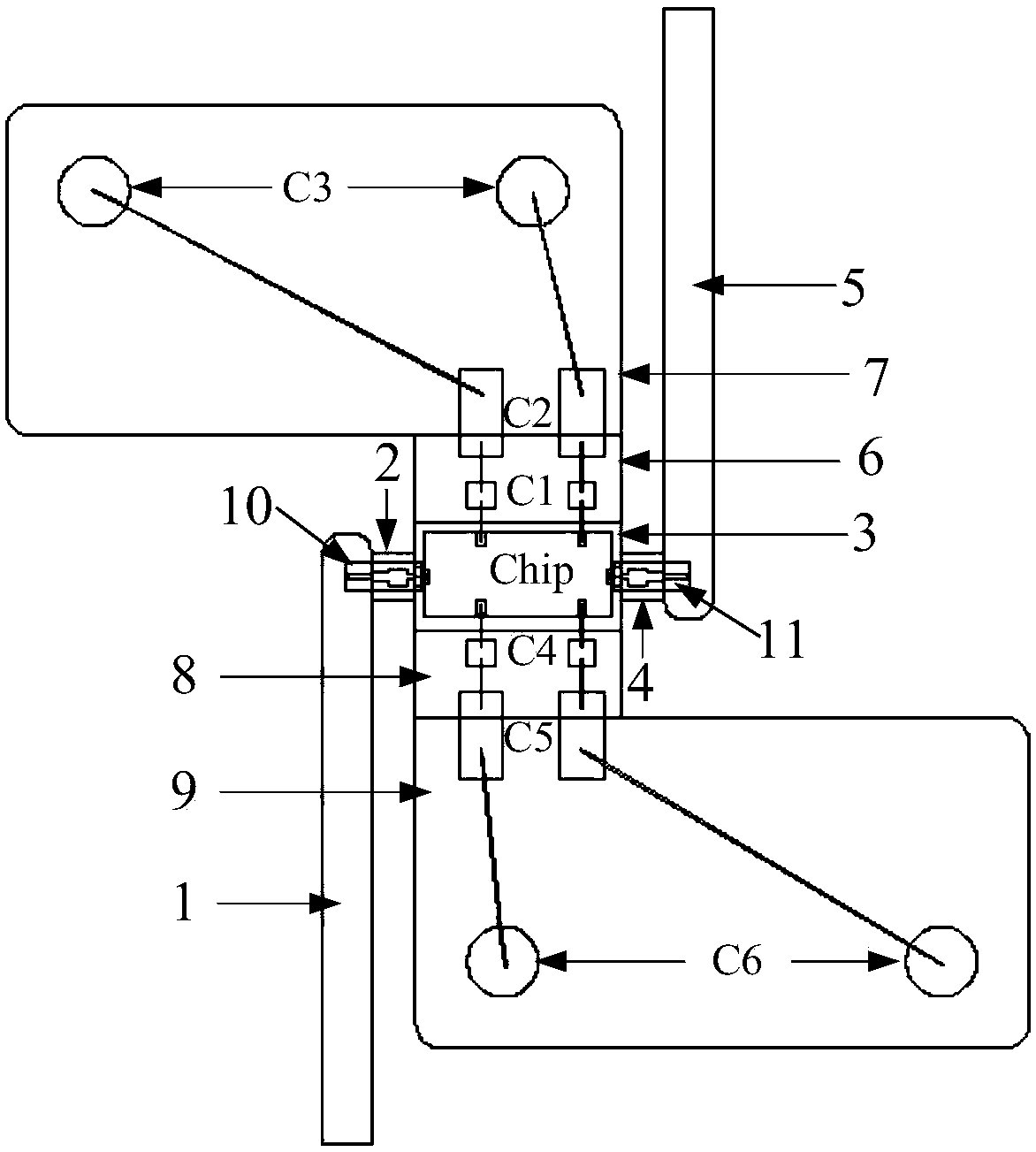
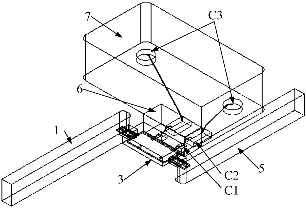
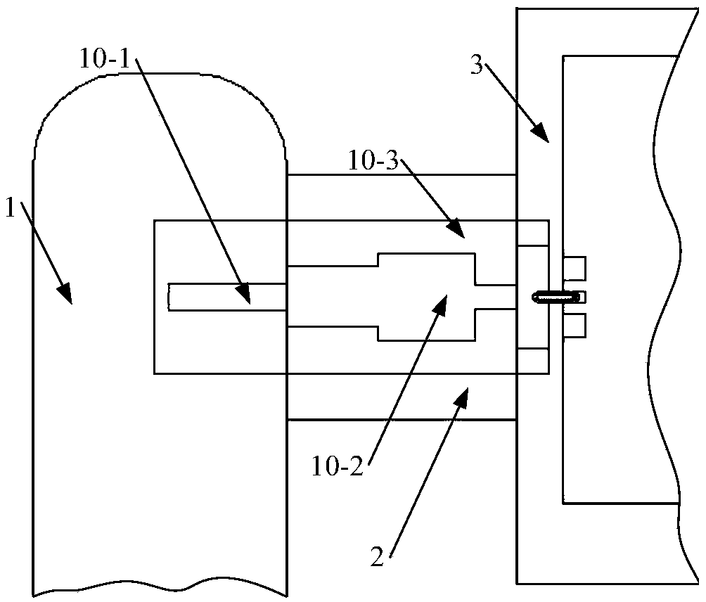
[0025] Such as figure 1 and figure 2 As shown, a millimeter-wave amplifier chip test cavity includes an input interface cavity 1, a microstrip probe matching structure loading cavity 2 at the input end, a millimeter-wave amplifier chip loading cavity 3, and a microstrip probe matching structure at the output end The loading cavity 4, the output interface cavity 5, the first capacitor combined cavity and the second capacitor combined cavity. The millimeter-wave amplifier chip test cavity is realized by computer-aided metal cavity processing technology, and is processed on brass material.

[0026] The input interface cavity 1, the input microstrip probe matching structure loading cavity 2, the millimeter wave amplifier chip loading cavity 3, the output microstrip probe matching structure loading cavity 4 and the output interface cavity 5 are connected in sequence , to rea...


PUM


Abstract

The invention discloses a millimeter wave amplifier chip testing cavity and method. Existing coaxial-interface-based millimeter wave amplifier chip testing devices only reaches a maximum working frequency of 145 GHz and fails to meet the testing and modularizing demands of high-frequency millimeter wave amplifier chips and to be applied to a millimeter wave front-end system. The millimeter wave amplifier chip testing cavity comprises an input interface cavity, an input end microstrip probe matching structure loading cavity, a millimeter wave amplifier chip loading cavity, an output end microstrip probe matching structure loading cavity, an output interface cavity, a first capacitor combination cavity and a second capacitor combination cavity, wherein the first capacitor combination cavityand the second capacitor combination cavity are arranged o both sides of the millimeter wave amplifier chip testing cavity. According to the millimeter wave amplifier chip testing cavity, the bias voltage of a millimeter frequency amplifier chip can be applied to independent power supply or by-pass capacitor filtering, thereby simplifying the structure and improving the circuit stability.

Description

technical field [0001] The invention belongs to the technical field of test cavity structure in microwave and millimeter wave chip circuits, and in particular relates to a test cavity for realizing a millimeter wave amplifier chip based on computer-aided metal cavity processing technology. Background technique [0002] In recent years, with the rapid development of wireless communication technology and the widespread use of various wireless terminals, high-speed wireless communication technology has put forward higher requirements for larger bandwidth and spectrum resources. The millimeter-wave frequency band has attracted widespread attention because of its wide bandwidth, large capacity, and easy miniaturization of the realized system. It has broad application prospects in the fifth and next generation wireless communications. The development of millimeter wave wireless communication technology is particularly important under the trend that the frequency utilization rate o...

Claims


Application Information

Patent Timeline
IPC IPC(8): G01R31/28H04B17/13H04B17/17
CPCG01R31/2844H04B17/13H04B17/17
Inventor 文进才杨丹丹何美林
Owner HANGZHOU DIANZI UNIV
Why Eureka
Try Eureka