
Etching method and semiconductor device

An etching gas, technology to be etched, used in semiconductor devices, semiconductor/solid-state device manufacturing, electrical solid-state devices, etc., and can solve problems such as removal

Active Publication Date: 2019-03-26
SHANGHAI HUALI MICROELECTRONICS CORP
View PDF7 Cites 4 Cited by
  • Summary
  • Abstract
  • Description
  • Claims
  • Application Information

AI Technical Summary

Problems solved by technology

Since the above-mentioned polymer shell layer 8 cannot be removed in subsequent etching and ashing processes, it will become a source of defects in subsequent processes

Method used


Image

  • Etching method and semiconductor device
  • Etching method and semiconductor device
  • Etching method and semiconductor device

Examples


Embodiment Construction

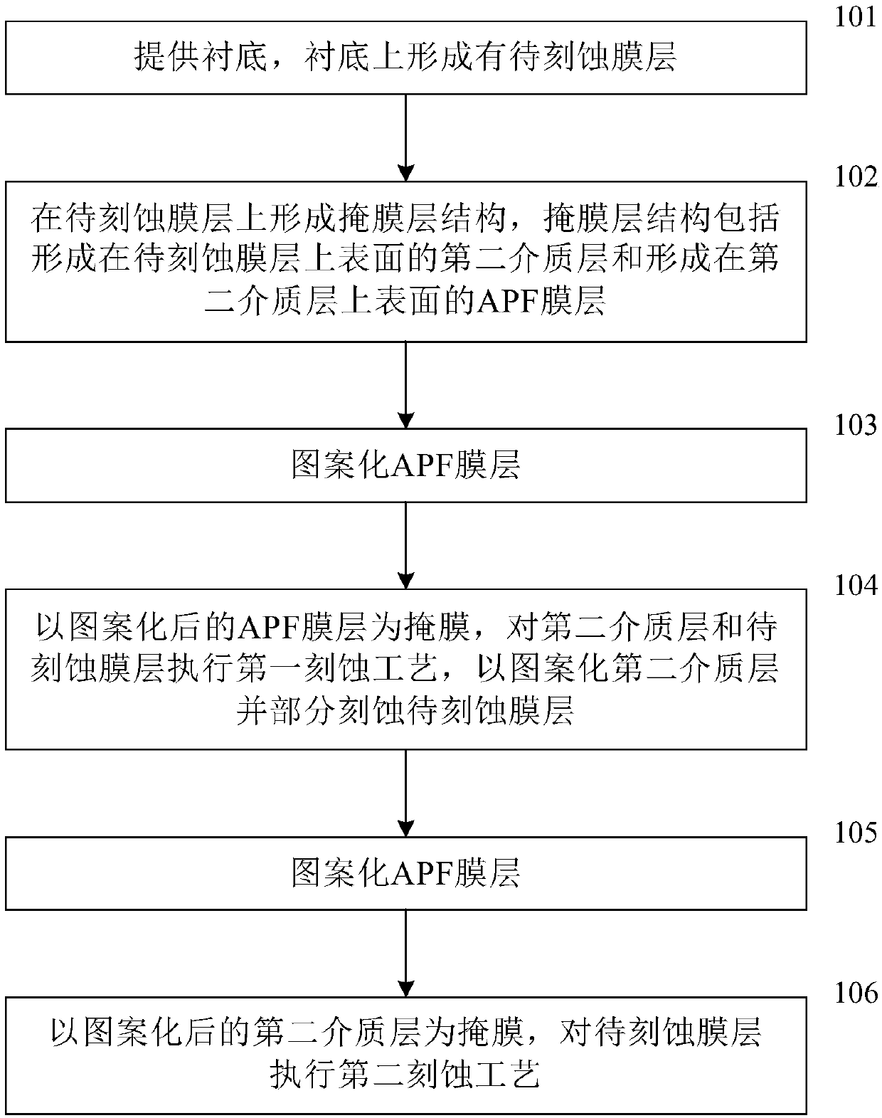
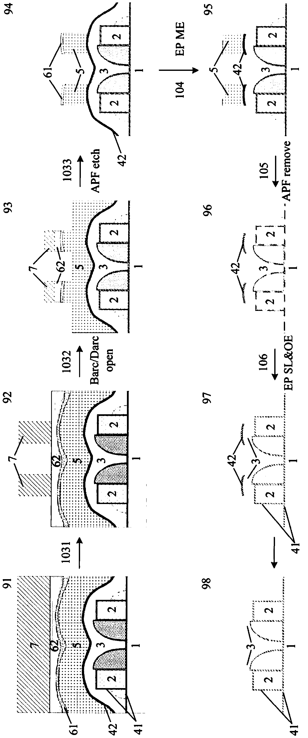
[0065] The implementation of the present invention will be illustrated by specific specific examples below, and those skilled in the art can easily understand other advantages and effects of the present invention from the content disclosed in this specification. Although the description of the invention will be presented in conjunction with a preferred embodiment, it is not intended that the features of the invention be limited to that embodiment only. On the contrary, the purpose of introducing the invention in conjunction with the embodiments is to cover other options or modifications that may be extended based on the claims of the present invention. The following description contains numerous specific details in order to provide a thorough understanding of the present invention. The invention may also be practiced without these details. Also, some specific details will be omitted from the description in order to avoid obscuring or obscuring the gist of the present inventio...


PUM

PropertyMeasurementUnit
Thicknessaaaaaaaaaa

Abstract

The invention belongs to the field of etching processing of semiconductor devices, and specifically discloses an etching method and a semiconductor device. The etching method includes: providing a substrate on which a film layer to be etched is formed; forming a mask layer structure on the film layer to be etched, wherein the mask layer structure includes a dielectric layer formed in the upper surface of the film layer to be etched and an APF film layer formed in the upper surface of the dielectric layer; patterning the APF film layer; by using the patterned APF film layer as a mask, performing a first etching process on the dielectric layer and the film layer to be etched so as to pattern the dielectric Layer and partially etch the film layer to be etched; removing the patterned APF filmlayer; and performing a second etching process on the film layer to be etched by using the patterned dielectric layer as a mask. The method can avoid the enrichment of a polymer generated in a polycrystalline silicon etching process on the surface of the APF, so as to eliminate defects of a polymer shell layer on the surface of the semiconductor device.

Description

technical field [0001] The invention relates to the field of etching processing of semiconductor devices, in particular to an etching method and a semiconductor device formed by the above etching method. Background technique [0002] With the continuous shrinking of semiconductor process nodes, the importance of hard mask etching for small-size polysilicon etching has become increasingly prominent. APF hard mask etching is due to its excellent line roughness (LER, Line Edge Roughness) performance, and for The high selectivity ratio of common etching film layers is widely used in polysilicon etching process. [0003] In a flash memory etching process with a novel structure, the erasing gate polysilicon (EP, Erase Polysilicon) etching process uses the APF as a hard mask to perform polysilicon etching. Due to the high step difference in the etched film layer structure, it is necessary to have a high amount of polysilicon etching in some areas. In addition, in order to protect...

Claims


Application Information

Patent Timeline
IPC IPC(8): H01L21/28H01L27/11521H01L27/11568
CPCH01L29/40114H01L29/40117H10B41/30H10B43/30H01L21/32139H01L29/4011H01L21/3081H01L21/31056H01L21/31144H01L21/32135
Inventor 韩朋刚许鹏凯
Owner SHANGHAI HUALI MICROELECTRONICS CORP
Learn More