A light-emitting diode epitaxial wafer and its manufacturing method

A technology of light-emitting diodes and manufacturing methods, applied to semiconductor devices, electrical components, circuits, etc., can solve the problems of reduced LED luminous efficiency, reduced hole injection efficiency, and difficulty in injecting into multi-quantum well light-emitting regions, etc., to reduce the density of dangling bonds , reduce the surface defect density, reduce the effects of leakage channels and non-radiative recombination centers

Active Publication Date: 2020-04-14
HC SEMITEK ZHEJIANG CO LTD
View PDF7 Cites 0 Cited by
  • Summary
  • Abstract
  • Description
  • Claims
  • Application Information

AI Technical Summary

Problems solved by technology

[0005] Due to the spontaneous polarization inside the GaN material, induced negative charges will appear on the upper surface of GaN, and these induced negative charges will cause the energy band on the GaN surface to bend upwards. In the LED epitaxial wafer, the upward-bent valence band on the upper surface of the P-type GaN layer For holes, it is a "potential energy valley". Part of the holes will be confined in this "potential energy valley". It is difficult to inject into the multi-quantum well light-emitting area, which reduces the hole injection efficiency, thereby reducing the luminous efficiency of the LED.

Method used


Image

  • A light-emitting diode epitaxial wafer and its manufacturing method
  • A light-emitting diode epitaxial wafer and its manufacturing method

Examples


Embodiment Construction

[0026] In order to make the object, technical solution and advantages of the present invention clearer, the implementation manner of the present invention will be further described in detail below in conjunction with the accompanying drawings.

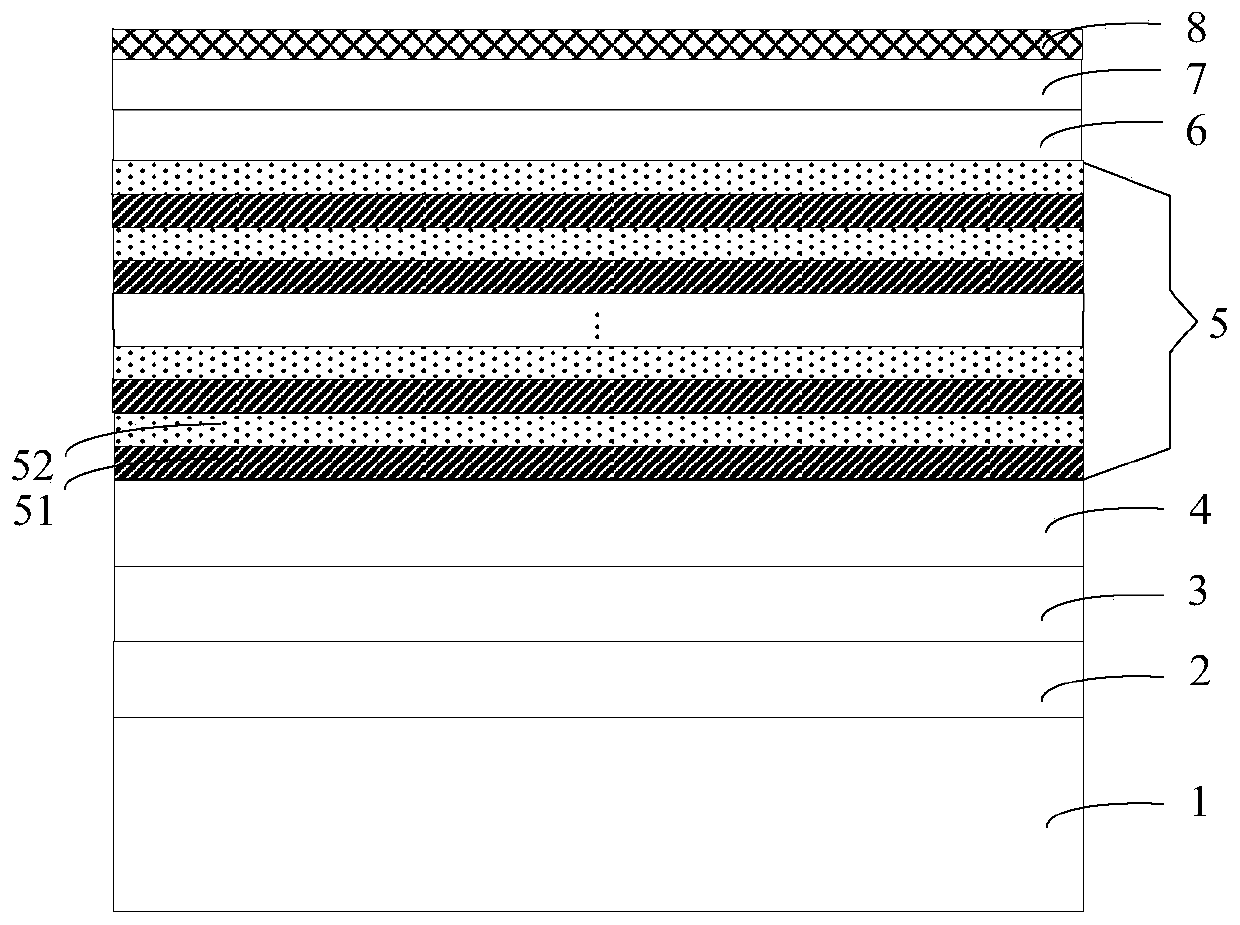
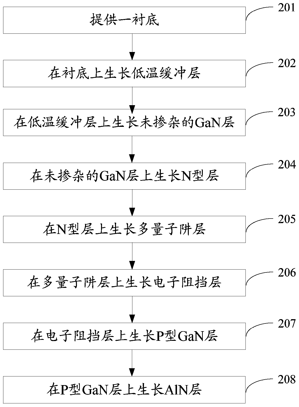
[0027] An embodiment of the present invention provides a light emitting diode epitaxial wafer, figure 1 It is a schematic structural diagram of a light-emitting diode epitaxial wafer provided by an embodiment of the present invention, as shown in figure 1 As shown, the light-emitting diode epitaxial wafer includes a substrate 1, and a low-temperature buffer layer 2, an undoped GaN layer 3, an N-type layer 4, a multi-quantum well layer 5, an electron blocking layer 6 and P-type GaN layer 7 .

[0028] The light emitting diode epitaxial wafer also includes an AlN layer 8 disposed on the P-type GaN layer 7 .

[0029] In the embodiment of the present invention, the AlN layer is grown on the P-type GaN layer. The band gap of the AlN materi...


PUM

PropertyMeasurementUnit
thicknessaaaaaaaaaa
thicknessaaaaaaaaaa
temperatureaaaaaaaaaa

Abstract

The invention discloses a light-emitting diode (LED) epitaxial wafer and a manufacturing method thereof and belongs to the technical field of semiconductors. The light-emitting diode epitaxial wafer comprises a substrate and also comprises a low-temperature buffer layer, an undoped GaN layer, an N-type layer, a multiple-quantum well layer, an electron blocking layer and a P-type GaN layer which are sequentially stacked on the substrate, and the light-emitting diode epitaxial wafer further comprises an AlN layer arranged on the P-type GaN layer. The forbidden bandwidth of the AlN material is larger than that of the GaN material. After the AlN layer is grown on an upper surface of the P-type GaN layer, the Fermi levels of two materials are aligned, an energy band on the upper surface of theP-type GaN layer is regulated, the bending direction of the upper surface of the P-type GaN layer changes from upward to downward, an original hole potential energy valley at that position disappears,the hole is not limited to the surface anymore, therefore, the movement of the hole to the direction of a multiple-quantum well is promoted, the injection efficiency of the hole is improved, and therefore, the luminous efficiency of an LED is improved.

Description

technical field [0001] The invention relates to the technical field of semiconductors, in particular to a light-emitting diode epitaxial wafer and a manufacturing method thereof. Background technique [0002] LED (Light Emitting Diode, Light Emitting Diode) is a semiconductor electronic component that can emit light. As an efficient, environmentally friendly and green new solid-state lighting source, it is being rapidly and widely used, such as traffic lights, car interior and exterior lights, urban landscape lighting, mobile phone backlights, etc. [0003] Epitaxial wafers are the main components of LEDs. The existing GaN-based LED epitaxial wafers include substrates and low-temperature buffer layers stacked on the substrates, undoped GaN layers, N-type layers, multiple quantum well layers, electronic barrier layer and P-type layer. The N-type layer is a GaN layer doped with Si, which can provide electrons, and the P-type layer is a GaN layer doped with Mg, which can prov...

Claims


Application Information

Patent Timeline
Patent Type & Authority Patents(China)
IPC IPC(8): H01L33/14H01L33/06H01L33/32H01L33/00
CPCH01L33/0066H01L33/0075H01L33/06H01L33/14H01L33/32
Inventor 唐成双李昱桦张燕飞刘春杨胡加辉
Owner HC SEMITEK ZHEJIANG CO LTD
Why Eureka
Try Eureka