Optimization method for large-power green-light LED epitaxial structure of Si substrate
A technology of epitaxial structure and optimization method, which is applied in the direction of electrical components, circuits, semiconductor devices, etc., can solve the problems of less than 40% external quantum efficiency, unsatisfactory development of green LED, and limited effect, so as to alleviate the decline of quantum efficiency, Effect of reducing carrier leakage and reducing polarization electric field
- Summary
- Abstract
- Description
- Claims
- Application Information
AI Technical Summary
Problems solved by technology
Method used
Image

Examples
Embodiment 1
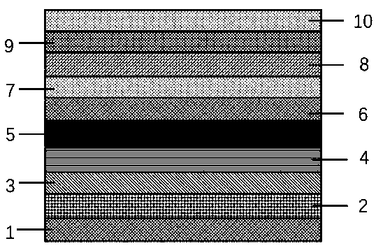
[0030] This embodiment provides a method for optimizing the epitaxial structure of a high-power green LED on a Si substrate, which is grown in an MOCVD system, using TMAl, TMGa, NH 3 and CP 2 Mg is used as Al source, Ga source, N source and Mg dopant respectively, H 2 as a carrier gas. The method for optimizing the epitaxial structure of high-power green LEDs on Si substrates specifically includes the following steps:
[0031] (1-1) Clean the purchased Si substrate (Si(111)) with a thickness of 800 microns in ethanol, acetone and deionized water for 20 minutes, dry it at 100°C and place it in a MOCVD glove box, and then use a suction cup to move the substrate Go to the substrate tray in the reaction chamber, raise the surface temperature of the epitaxial wafer to 1050°C in a hydrogen atmosphere, heat treat for 5 minutes to completely remove the surface oxide, and obtain Si substrate 1;
[0032] (1-2) Cool down the reaction chamber to 1000°C, first pass trimethylaluminum TMA...
Embodiment 2
[0047] This embodiment provides a method for optimizing the epitaxial structure of a high-power green LED on a Si substrate, which is grown in an MOCVD system, using TMAl, TMGa, NH 3 and CP 2 Mg is used as Al source, Ga source, N source and Mg dopant respectively, H 2 as a carrier gas. Specifically include the following steps:
[0048] (2-1) Clean the purchased Si substrate (Si(111)) with a thickness of 800 microns in ethanol, acetone and deionized water for 30 minutes, dry it at 80°C and place it in the MOCVD glove box, and then use the suction cup to move the substrate Go to the substrate tray in the reaction chamber, raise the surface temperature of the epitaxial wafer to 1100°C in a hydrogen atmosphere, heat treat for 5 minutes to completely remove the surface oxide, and obtain Si substrate 1;
[0049] (2-2) Cool down the reaction chamber to 1000°C, first pass TMAl for 10s, and then pass NH 3 , the pressure is 200 mbar, the V / III molar ratio is 400, and a medium-temper...
Embodiment 3
[0063] In this embodiment, a method for optimizing the epitaxial structure of a high-power green LED on a Si substrate is grown in an MOCVD system, using TMAl, TMGa, NH 3 and CP 2 Mg is used as Al source, Ga source, N source and Mg dopant respectively, H 2 as a carrier gas. Specifically include the following steps:
[0064] (3-1) Clean the purchased Si substrate (Si(111)) with a thickness of 800 microns in ethanol, acetone and deionized water for 30 minutes, dry it at 90°C and place it in a MOCVD glove box, and then use a suction cup to move the substrate Go to the substrate tray in the reaction chamber, raise the surface temperature of the epitaxial wafer to 1100°C in a hydrogen atmosphere, heat treat for 3 minutes to completely remove the surface oxide, and obtain Si substrate 1;
[0065] (3-2) Cool down the reaction chamber to 900°C, first pass TMAl for 15s, and then pass NH 3 , the pressure is 300 mbar, the V / III molar ratio is 500, and a medium-temperature AlN buffer ...
PUM
| Property | Measurement | Unit |
|---|---|---|
| Thickness | aaaaa | aaaaa |
| Thickness | aaaaa | aaaaa |
| Thickness | aaaaa | aaaaa |
Abstract
Description
Claims
Application Information
 - R&D
- Intellectual Property
- Life Sciences
- Materials
- Tech Scout
- Unparalleled Data Quality
- Higher Quality Content
- 60% Fewer Hallucinations
Browse by: Latest US Patents, China's latest patents, Technical Efficacy Thesaurus, Application Domain, Technology Topic, Popular Technical Reports.
© 2025 PatSnap. All rights reserved.Legal|Privacy policy|Modern Slavery Act Transparency Statement|Sitemap|About US| Contact US: help@patsnap.com