Field emission electrode and preparation method thereof

A field emission and electrode technology, which is applied in the manufacture of electrode systems, cold cathodes, discharge tubes/lamps, etc., can solve the problems of unsuitable large-area field emission electrode array preparation, immature controllable growth technology, growth Expensive and other issues, to achieve the effect of simple and mild growth conditions, enhanced emission performance, and improved emission performance

Active Publication Date: 2019-04-05
SHENZHEN INST OF ADVANCED TECH
View PDF7 Cites 8 Cited by
  • Summary
  • Abstract
  • Description
  • Claims
  • Application Information

AI Technical Summary

Problems solved by technology

[0004] At present, the nanowires in the field emission electrodes of field emission devices are mainly prepared and formed on the patterned electrode layer on the support plate by chemical vapor

Method used


Image

  • Field emission electrode and preparation method thereof
  • Field emission electrode and preparation method thereof
  • Field emission electrode and preparation method thereof

Examples


Embodiment Construction

[0029] In order to make the objectives, technical solutions, and advantages of the present invention clearer, the specific embodiments of the present invention will be described in detail below with reference to the accompanying drawings. Examples of these preferred embodiments are illustrated in the drawings. The embodiments of the present invention shown in the drawings and described in accordance with the drawings are merely exemplary, and the present invention is not limited to these embodiments.

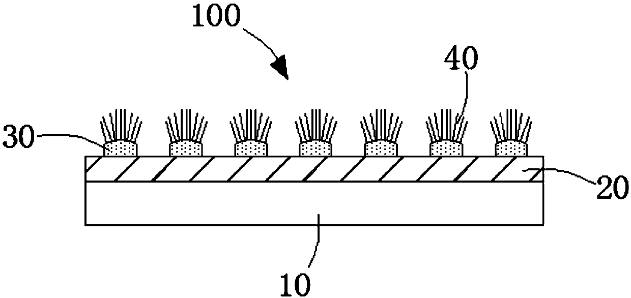
[0030] This embodiment first provides a field emission electrode, such as figure 1 As shown, the field emission electrode 100 includes a substrate 10 and a metal electrode layer 20 formed on the substrate 10. The metal electrode layer 20 is provided with a plurality of indium pillars 30 arranged in an array. The top surface of the indium column 30 is provided with a plurality of nanowires 40.

[0031] In the above electrode structure, an array of indium pillars 30 are arranged on th...


PUM

PropertyMeasurementUnit
Heightaaaaaaaaaa
Diameteraaaaaaaaaa
Thicknessaaaaaaaaaa

Abstract

The invention discloses a field emission electrode. The field emission electrode comprises a substrate and a metal electrode layer formed on the substrate, the metal electrode layer is provided with aplurality of indium bumps arranged in an array, and the top surface of each indium bump is provided with a plurality of nanowires. The preparation method comprises the steps of: S10, providing a substrate, and performing depositing on the substrate to form a metal electrode layer; S20, preparing a photoresist mask having a hole array on the metal electrode layer; S30, depositing indium materialson the photoresist mask to peel off the photoresist mask to obtain the indium bumps arranged in the array; and S40, putting the substrate with the formed indium bumps in a reaction furnace, wherein the top surface of each indium bump grows and forms the plurality of nanowires. The field emission electrode has an excellent field emission performance and is simple in preparation process, the growthof the nanowires can be performed in the low temperature and the low voltage, the growth condition is simple and gentle and easy to control, and therefore, the quality of products can be effectively improved and the production cost is reduced.

Description

Technical field [0001] The invention belongs to the technical field of field emission devices, and particularly relates to a field emission electrode and a preparation method thereof. Background technique [0002] Nanomaterials refer to materials with a size roughly in the range of 1~300nm. A series of effects such as surface effects, small size effects, quantum size effects and macroscopic quantum tunneling effects are easily produced at this scale. These effects make nanomaterials possess In addition to the special properties that macroscopic objects do not possess, it shines in various fields such as: electrochemistry, sensors, field emission devices and other fields. [0003] Field emission devices are widely used as electron sources for microwave elements, sensors, flat panel display devices, and the like. When an electric field is applied to the cathode electrode in a vacuum or a specific atmosphere, the field emission device emits electrons from the cathode electrode. In a ...

Claims


Application Information

Patent Timeline
IPC IPC(8): H01J1/304H01J9/02B82Y30/00B82Y40/00
CPCB82Y30/00B82Y40/00H01J1/3044H01J9/025
Inventor 张道书陈明洪序达冯叶钟国华李文杰杨春雷
Owner SHENZHEN INST OF ADVANCED TECH
Why Eureka
Try Eureka