Supercharge Your Innovation With Domain-Expert AI Agents!

Coupling packaging structure and method of single mode fiber and silicon-based photo-electronic chip end face

An optoelectronic chip, single-mode fiber technology, applied in the coupling of optical waveguides, light guides, optics, etc., can solve the problems of large surface area, high energy loss, huge loss, etc., to achieve large surface area, improve efficiency, and improve coupling redundancy. Effect

Inactive Publication Date: 2019-04-12
UNITED MICROELECTRONICS CENT CO LTD
View PDF9 Cites 7 Cited by
  • Summary
  • Abstract
  • Description
  • Claims
  • Application Information

AI Technical Summary

Problems solved by technology

[0004] In order to solve the problems that the existing coupling and packaging methods of single-mode optical fiber and silicon-based optoelectronic chip end faces have huge losses, etc., the present invention innovatively provides a coupling packaging structure and method for single-mode optical fiber and silicon-based optoelectronic chip end faces. Optical fiber with special structure and coupling package structure. The present invention can effectively match the optical fiber and the end face of the silicon-based optoelectronic chip, which not only greatly reduces the energy loss of end face coupling, but also has the advantages of high coupling efficiency and easy packaging. The field of semiconductor packaging has broad application prospects
[0006] Based on the above technical solution, the present invention innovatively uses the high numerical aperture optical fiber as the optical fiber directly coupled with the silicon-based optoelectronic chip, thereby solving the problem of excessive energy loss in the existing coupling method, and the present invention can match the optical fiber and the electronic chip through a stepped structure The height of the waveguide is provided by the fiber capillary for stress clamping in the coupling process and stress support in the packaging process. The fiber capillary is convenient to be reliably clamped by fixtures such as a six-axis adjustment frame. Stabilize the optical fiber during the alignment process, improve alignment efficiency and accuracy; and the surface area of ​​the optical fiber capillary is large, which can achieve more effective and reliable fixation with the base plate

Method used


Image

  • Coupling packaging structure and method of single mode fiber and silicon-based photo-electronic chip end face
  • Coupling packaging structure and method of single mode fiber and silicon-based photo-electronic chip end face
  • Coupling packaging structure and method of single mode fiber and silicon-based photo-electronic chip end face

Examples


Embodiment 1

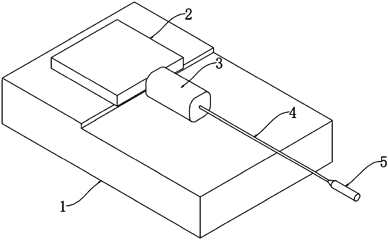
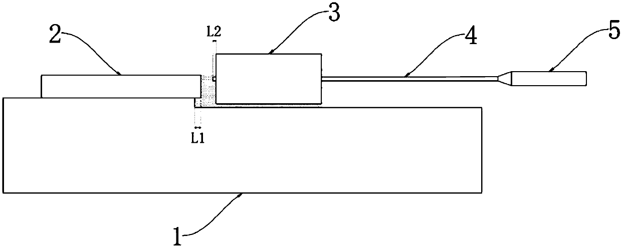
[0047] Such as Figures 1 to 5As shown, this embodiment discloses a coupling packaging structure of a single-mode optical fiber and an end face of a silicon-based optoelectronic chip. The coupling packaging structure includes a base plate 1, a silicon-based optoelectronic chip 2, an optical fiber capillary 3, a high numerical aperture optical fiber 4 and a single-mode optical fiber 5 It should be understood that the numerical aperture (NA) range of the high numerical aperture optical fiber 4 involved in the present invention is 0.28~0.41, and the high numerical aperture optical fiber 4 can select UHNA1 (NA: 0.28, core diameter 2.5 μ m:) or UHNA3 (NA : 0.35, core diameter: 1.8 μm) or UHNA4 (NA: 0.35, core diameter: 2.2 μm) or UHNA7 (NA: 0.41, core diameter: 2.4 μm); in this embodiment, the selected high numerical aperture fiber The model of 4 is UHNA7, and the high numerical aperture optical fiber 4 has two ends. In this embodiment, the two ends of the high numerical aperture o...

Embodiment 2

[0054] Based on the same inventive concept as Embodiment 1, this embodiment discloses a coupling and packaging method for a single-mode optical fiber and the end face of a silicon-based optoelectronic chip, based on an optical fiber with a special structural design (an optical fiber formed after fusion of a high numerical aperture optical fiber and a single-mode optical fiber ), through end-face coupling between one end of the high numerical aperture optical fiber and the silicon-based optoelectronic chip, thereby providing a highly stable packaging method for the single-mode fiber and the end face of the silicon-based optoelectronic chip, specifically, as Figure 6 As shown, the coupling and packaging method includes the following steps.

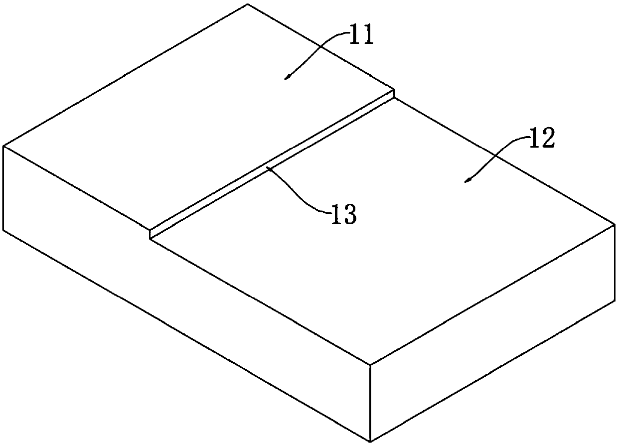
[0055] Step 1, fusion splicing and fiber capillary setting steps: fusion splicing end 41 of high numerical aperture optical fiber 4 and one end of single mode optical fiber 5, and after the two are fused, a gradual tapered shape is formed at...


PUM


Abstract

The invention discloses a coupling packaging structure and method of a single mode fiber and a silicon-based photo-electronic chip end face. The structure comprises a bottom plate, a silicon-based photo-electronic chip, an optical fiber capillary, a high-numerical aperture fiber, and the single mode fiber. Two ends of the high-numerical aperture fiber are separately connected with the silicon-based photo-electronic chip and the single mode fiber. The silicon-based photo-electronic chip and the optical fiber capillary are fixed to the bottom plate. The method comprises the following steps thatwelding and optical fiber capillary arranging are conducted, step etching and chip fixing are conducted, coupling is conducted, ultraviolet adhesive filling is conducted, and solidification is conducted. Compared with the prior art, the high-numerical aperture fiber is adopted as an energy transmission medium of the single mode fiber and the silicon-based photo-electronic chip, and the existing problem of coupled mode spot mismatch between single mode fiber and the silicon-based photo-electronic chip is solved. Coupling with minimal energy loss is achieved. The coupling packaging structure andmethod have the advantages of being high is stability, high in coupling efficiency and simple in packaging, and having a wide application prospect.

Description

technical field [0001] The invention relates to the technical field of single-mode optical fiber and silicon-based optoelectronic chip packaging, more specifically, the invention relates to a coupling packaging structure and method for a single-mode optical fiber and a silicon-based optoelectronic chip end face. Background technique [0002] In recent years, silicon-based optoelectronics has been greatly developed, because the manufacturing process of silicon-based integrated optical devices is fully compatible with microelectronics technology, and the carrier light wave transmitted in silicon-based optoelectronic chips is a kind of extremely high frequency, which can provide The transmission of the signal provides electromagnetic waves of extremely high bandwidth. However, since the mode spot diameter of the optical field in the end face waveguide of the silicon-based optoelectronic chip is 3.5 μm, and the core diameter of the single-mode fiber is generally relatively large...

Claims


Application Information

Patent Timeline
Patent Type & Authority Applications(China)
IPC IPC(8): G02B6/42G02B6/255
CPCG02B6/2551G02B6/4239G02B6/4244G02B6/4245
Inventor 赵恒金里何来胜冯俊波
Owner UNITED MICROELECTRONICS CENT CO LTD
Features
  • R&D
  • Intellectual Property
  • Life Sciences
  • Materials
  • Tech Scout
  • Unparalleled Data Quality
  • Higher Quality Content
  • 60% Fewer Hallucinations
Learn More