Compounding and forming integrated device and method for multi-layer metal micro-channel structure

A micro-channel structure and micro-channel technology, applied in metal processing equipment, forming tools, manufacturing tools, etc., can solve the problems of micro-channel research with strict operation requirements, not suitable for the field of metal materials, complex structure of preparation devices, etc. The effect of short process flow, reduction of material deformation resistance and friction coefficient, and simple device structure

Active Publication Date: 2019-04-19
HARBIN INST OF TECH AT WEIHAI
View PDF15 Cites 4 Cited by
  • Summary
  • Abstract
  • Description
  • Claims
  • Application Information

AI Technical Summary

Problems solved by technology

[0004] Chinese patent document CN102411060A (patent application number 201110401804.9) discloses a microfluidic chip with a high aspect ratio microfluidic channel and its manufacturing method. The material is polydimethylsiloxane (PDMS), And it is made by soft lithography technology, and the male mold used in the casting of the microfluidic chip is processed by SU-8 maskless lithography. Although this technology has the advantages of high flexibility, low production cost and short cycle, its preparation The structure of the device is complex, the operation requirements are strict, and it is not suitable for the research of microchannels in the field of metal materials

Method used


Image

  • Compounding and forming integrated device and method for multi-layer metal micro-channel structure
  • Compounding and forming integrated device and method for multi-layer metal micro-channel structure

Examples


Embodiment Construction

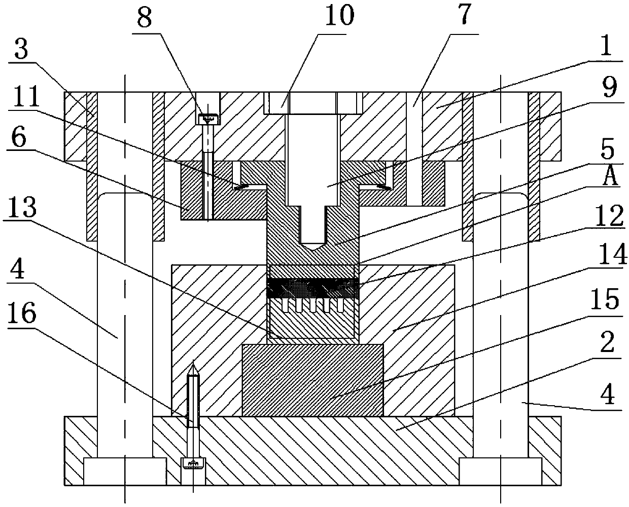
[0025] The present invention will be further described below in conjunction with the accompanying drawings and specific embodiments, so as to help understand the content of the present invention. The methods used in the present invention are conventional methods unless otherwise specified; the raw materials and devices used are conventional commercially available products unless otherwise specified.

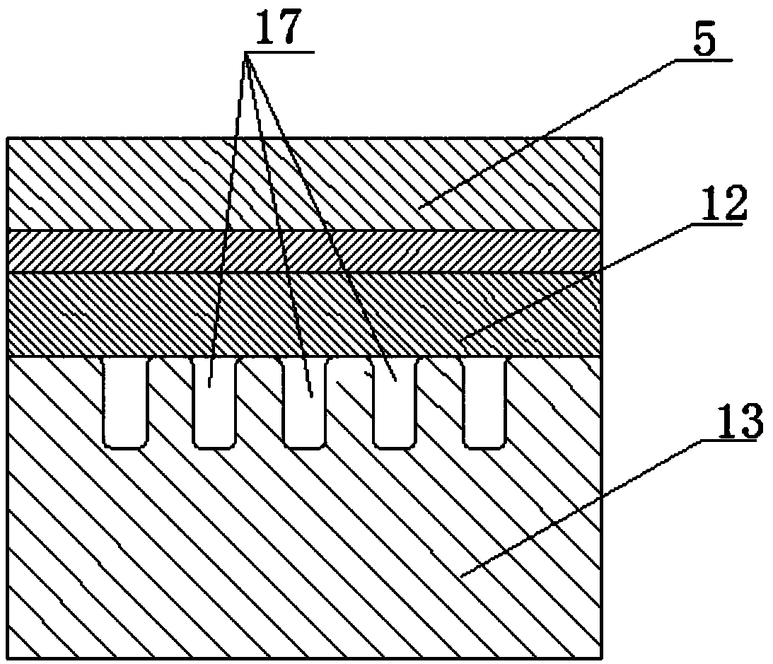
[0026] like Figure 1-Figure 2 As shown, the present invention provides an integrated device for compounding and forming of a multilayer metal microchannel structure, including a matching upper mold base 1 and a lower mold base 2, and the upper mold base 1 and the lower mold base 2 pass through the guide sleeve 3 and the guide post 4 are connected to form a closed frame structure. The upper mold base 1 can realize up and down reciprocating movement through the guide sleeve 3 and the guide column 4; the guidance between the upper template 1 and the lower template 2 is guaranteed b...


PUM

PropertyMeasurementUnit
widthaaaaaaaaaa
heightaaaaaaaaaa
thermal conductivityaaaaaaaaaa

Abstract

The invention discloses a compounding and forming integrated device and method for a multi-layer metal micro-channel structure. The device and method solve the technical problems that in existing structure design, a mold device is complex in structure, the machining process of the metal micro-channel structure is complex in procedure and high in manufacturing cost, a micro-channel structure formedby independent machining of mono-metal materials is poor in quality, and the performance of the structure is not improved. The compounding and forming integrated device comprises an upper mold base and a lower mold base which are matched; the upper mold base achieves vertical reciprocating movement through a guide sleeve and a guide column; a convex mold is fixedly arranged on the lower surface of the upper mold base; a concave mold is fixedly arranged on the upper surface of the lower mold base; the concave mold and a concave mold fixing board define a mold cavity; a micro-channel groove isformed in the upper surface of the concave mold in an inwards concave mode; the convex mold is fixedly arranged on the lower surface of the upper mold base through a convex mold fixing board; a grooveis formed in the position of the upper surface, making contact with the upper mold base, of the upper end of the convex mold in an inwards concave mode; a vibrator penetrating through the upper moldbase is fixedly connected with the interior of the groove; and the compounding and forming integrated device and method for the multi-layer metal micro-channel structure can be widely applied to the field of precision manufacturing of bi-metal micro-channel structures.

Description

technical field [0001] The invention belongs to the field of precision manufacturing of bimetallic microchannel structures, and in particular relates to an integrated device and method for compounding and forming a multilayer metal microchannel structure. Background technique [0002] With the continuous miniaturization of the structure of micro-miniature devices, the energy transport inside the device is limited by the tiny space, which makes high-power devices face the problem of high energy and rapid heat transport caused by excessive power. The problem of chip thermal control brought about by the temperature sensitivity of microelectronic devices has also been highlighted. The reliability of electronic devices is very sensitive to temperature. Any well-designed electronic device will fail or fail under the action of long-term overheating and uneven thermal stress. Generally, the operating temperature of electronic devices should be below 130°C. The famous 10°C rule poi...

Claims


Application Information

Patent Timeline
Patent Type & Authority Applications(China)
IPC IPC(8): B21D37/10B21D39/00
CPCB21D37/10B21D39/00
Inventor 王传杰张鹏陈刚栾冬郭斌
Owner HARBIN INST OF TECH AT WEIHAI
Why Eureka
Try Eureka