Crimp connection type IGBT internal package structure

An internal packaging and crimping technology, which is applied in the direction of semiconductor/solid-state device parts, electrical components, and electrical solid-state devices, can solve the problems of difficult mutual positioning, high chip loss rate, and complicated packaging process, etc., to achieve convenient module Minimized assembly, simplified packaging process, and good electrical conductivity

Pending Publication Date: 2019-04-19
XIAN YONGDIAN ELECTRIC
View PDF0 Cites 7 Cited by
  • Summary
  • Abstract
  • Description
  • Claims
  • Application Information

AI Technical Summary

Problems solved by technology

Among them, molybdenum sheet-IGBT / FRD chip-molybdenum sheet structure, molybdenum sheet-IGBT / FRD chip-molybdenum sheet-silver sheet structure, pressure-connected IGBT devices have more assembly components, and the thickness of the chip and silver sheet is relatively thin. Brittle, the material of the silver sheet is soft, it is difficult to achieve mutual positioning, the packaging process is more complicated, and the loss rate of the chip during the assembly process is relatively large
The molybdenum sheet-silver sintered layer-IGBT / FRD chip-molybdenum sheet-silver sheet structure first uses nano-silver solder to realize the sintering and fixing of the chip collector and the molybdenum sheet, and introduces the silver sintered layer as a pressure-bonding buffer layer, which is better than molybdenum sheet-IGBT / FRD chip-molybdenum sheet structure, molybdenum sheet-IGBT / FRD chip-molybdenum sheet-silver sheet structure have greatly improved the ease of assembly and chip loss rate, but the molybdenum sheet-silver sheet structure on the side of the emitter It has not changed, and there are also problems that mutual positioning is difficult to achieve, and the packaging process is more complicated.

Method used


Image

  • Crimp connection type IGBT internal package structure
  • Crimp connection type IGBT internal package structure
  • Crimp connection type IGBT internal package structure

Examples


Embodiment Construction

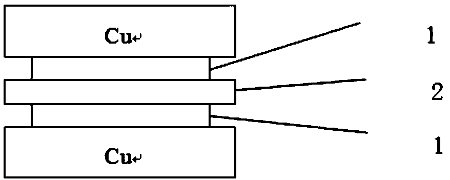
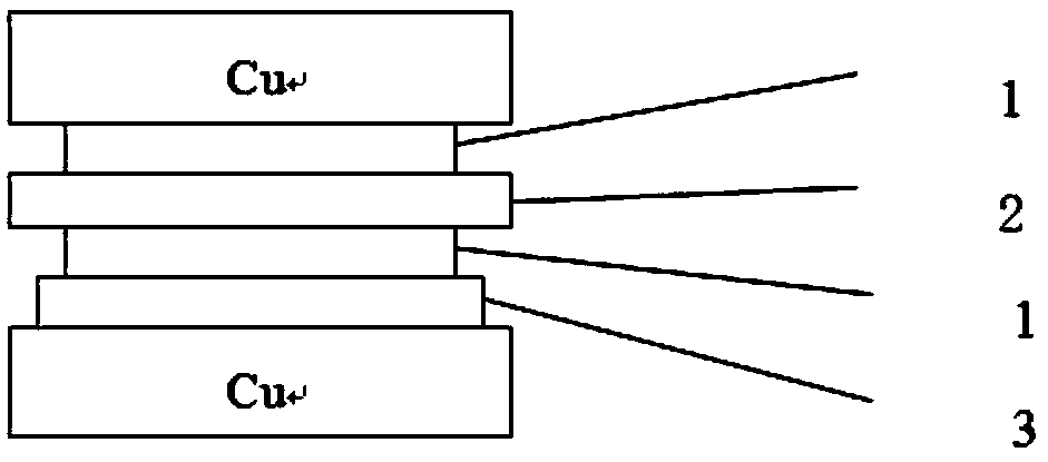
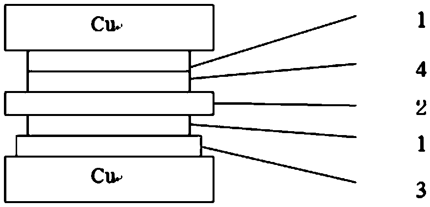
[0028] In order to simplify the packaging process of the ceramic shell press-fit IGBT and realize the development of the press-fit IGBT, the present invention has finally designed a new internal structure of the press-fit IGBT packaged in the ceramic shell through assiduous technical research. like Image 6 As shown, the structure specifically includes the IGBT / FRD chip 2 and the silicon carbide aluminum layer 9, the silicon carbide aluminum layer 9 is located on the upper and lower sides of the IGBT / FRD chip 2, and the IGBT / FRD chip 2 and the silicon carbide aluminum layer A solder layer 10 is provided between 9, and a metal layer 11 is provided on the upper and lower surfaces of the IGBT / FRD chip 2.

[0029] The present invention has obtained through several tests that the material of the metal layer 11 is preferably an Al / Ti / Ni / Ag four-layer integrated metal layer, and the thickness is preferably 2um-5um. Al / Ti / Ni / Ag four-layer integrated metal layer is prepared by traditi...


PUM


Abstract

The invention provides a crimp connection type IGBT internal package structure encapsulated in a ceramic tube casing. The structure comprises an IGBT/FRD chip and silicon carbide aluminum layers. Thesilicon carbide aluminum layers are located on the upper and lower sides of the IGBT/FRD chip. A soldering layer is arranged between the IGBT/FRD chip and each of the silicon carbide aluminum layers,and the upper and lower surfaces of the IGBT/FRD chip are provided with metal layers. The invention provides a silicon carbide aluminum-soldering layer-IGBT/FRD chip-welding layer-silicon carbide aluminum internal structure of a ceramic shell packaged crimp connection type IGBT, so the packaging process operation of the ceramic shell packaged crimp connection type IGBT is greatly simplified; double-sided heat dissipation of the crimp connection type IGBT is ensured; and requirement of high current flow and high reliability are met.

Description

technical field [0001] The invention belongs to the technical field of IGBT package structure, and in particular relates to a crimping type IGBT internal package structure capable of being packaged in a ceramic tube case. Background technique [0002] IGBT is a composite device of MOSFET and bipolar transistor. It not only has the characteristics of easy driving of MOSFET, but also has the characteristics of high voltage and high current of power transistor. It is recognized by the world as a representative product of the third technological revolution of power electronics. [0003] Compared with the soldered IGBT, the press-fit IGBT has the advantages of double-sided heat dissipation, wider safe operating area (SOA), higher operating junction temperature, no leads, high reliability, and special characteristics of short-circuit failure. In flexible DC The devices in the power transmission converter valve have a very significant competitive advantage in the application fields...

Claims


Application Information

Patent Timeline
Patent Type & Authority Applications(China)
IPC IPC(8): H01L23/02H01L23/10H01L29/739
CPCH01L23/02H01L23/10H01L29/7393
Inventor 王豹子屈斌叶娜黄小娟
Owner XIAN YONGDIAN ELECTRIC
Why Eureka
Try Eureka