

Silica-based high-current transfer ratio pair Darlington transistor and making method thereof
A manufacturing method and high-current technology, which are applied in the fields of electric solid-state devices, semiconductor/solid-state device manufacturing, circuits, etc., can solve the problems of increasing the amplification cost of subsequent circuits, the volume of the whole machine, low current transfer ratio, and low photoelectric response. Reduce the cost of amplification, solve the effect of lower photoelectric response and save volume
- Summary
- Abstract
- Description
- Claims
- Application Information
AI Technical Summary
Problems solved by technology
Method used
Image

Examples
Embodiment 1
[0034] Embodiment 1 Silicon-Based High Current Transfer Ratio Double Darlington Transistor
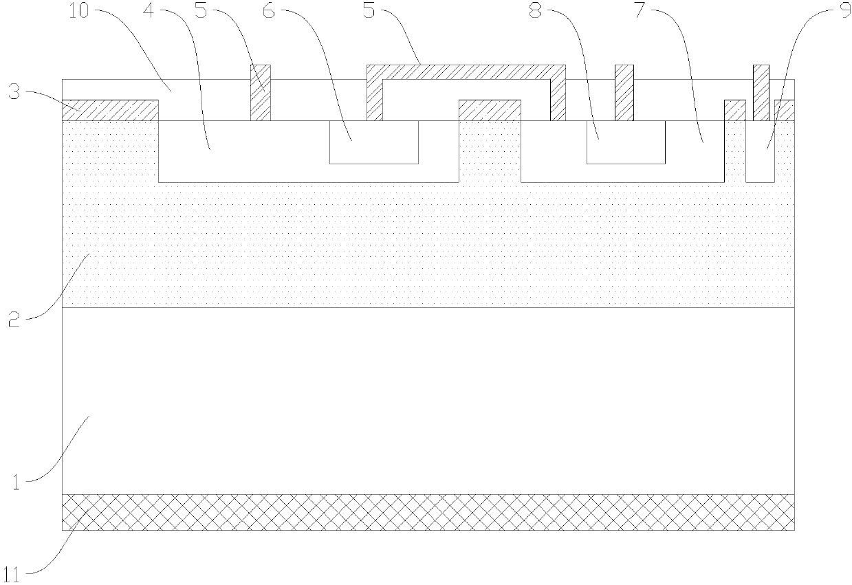
[0035] Such as Figure 1-4 As shown, a silicon-based high current transfer ratio double Darlington transistor in this embodiment includes a substrate layer 1, an N-type silicon epitaxial layer 2, a silicon dioxide passivation layer 3, a first base region 4, and an electrode 5. The first-level emitter region 6, the second-level base region 7, the second-level emitter region 8, the collector region 9, the silicon nitride layer 10 and the bottom electrode 11, wherein the first base region 4 is the photosensitive region The bottom electrode 11, the N-type silicon epitaxial layer substrate 1, the N-type silicon epitaxial layer 2, the silicon dioxide passivation layer 3, and the silicon nitride layer 10 are sequentially arranged from bottom to top, and the first base region 4 , the second-level base region 7 and the collector region 9 are arranged on the top of the N-type silicon epitaxial ...
Embodiment 2
[0036] Embodiment 2 Manufacturing method of silicon-based high current transmission ratio double Darlington transistor
[0037] In this embodiment silicon based high current transfer ratio dual Darlington transistors, such as figure 1 Shown, its preparation method comprises the following steps:
[0038] 1) The substrate layer 1 and the N-type silicon epitaxial layer 2 are formed by using N-type silicon epitaxial material, the resistivity of the N-type silicon epitaxial layer 2 is 20±5Ω·cm, and the thickness of the epitaxial layer is 20±5μm; the side where the epitaxial layer 2 is located The end face of the device is marked as the front face, and the end face of the device on the side where the substrate layer 1 is located is marked as the back face;
[0039] 2) Using a high-temperature oxidation process to form a silicon dioxide passivation layer 3 on the front surface of the device;
[0040] 3) Photoetching the first base region 4 and the second base region 7 on the front ...
Embodiment 3
[0048] Embodiment 3 Manufacturing method of silicon-based high current transmission ratio double Darlington transistor
[0049] The manufacturing method of the silicon-based high current transfer ratio double Darlington transistor in this embodiment includes the following steps:
[0050] 1) Use N-type silicon epitaxial materials to form the substrate layer and N-type silicon epitaxial layer. The resistivity of the N-type silicon epitaxial layer is 20±5Ω·cm, and the thickness of the epitaxial layer is 20±5μm; is the front side, and the device end face on the side where the substrate layer is located is marked as the back side;
[0051] 2) A high-temperature oxidation process is used to form a silicon dioxide passivation layer on the front surface of the device;
[0052] 3) Photoetching the first polar base region and the second-level base region on the front side of the device using a photolithography process; using a wet etching process to etch the silicon dioxide passivation...
PUM
| Property | Measurement | Unit |
|---|---|---|
| Thickness | aaaaa | aaaaa |
| Thickness | aaaaa | aaaaa |
| Thickness | aaaaa | aaaaa |
Abstract
Description
Claims
Application Information