Method for manufacturing flexible printed circuit board

A technology of flexible printing and manufacturing method, which is applied in the manufacture of printed circuits, printed circuits, and the removal of conductive materials by chemical/electrolytic methods. It can solve the problems of difficulty in improving reliability, poor spatial stability, and low wiring density. And the heat dissipation performance is improved, the thickness and strength are guaranteed, and the space stability is good.

Active Publication Date: 2019-04-26
邑升顺电子(深圳)有限公司
View PDF5 Cites 0 Cited by
  • Summary
  • Abstract
  • Description
  • Claims
  • Application Information

AI Technical Summary

Problems solved by technology

In this way, the solder bumps used for soldering are obviously protruded relative to the surface of the integrated flexible printed circuit board, which is easy to cause the integrated flexible printed circuit board to break at the welding position, resulting in the failure of the integrated flexible printed circuit board
[0004] Combining the above technical solutions and existing problems in reality, as well as combining the currently widely used technical solutions, the main defects are mainly reflected in the following aspects: poor thermal conductivity and heat dissipation, and difficult to control the transformation of the spatial structure and the specific size , which directly leads to its difficulty in improving its reliability; furthermore, because of the extremely poor dimensional stability and low wiring density, it is not convenient to make multilayer boards, and in the prior art, mechanical punching is used in the manufacture of multilayer flexible circuit boards. When the hole and mechanical cutting are used, it is easy to produce slag particles of various particle sizes, which will affect the performance of the circuit board

Method used


Image

  • Method for manufacturing flexible printed circuit board
  • Method for manufacturing flexible printed circuit board
  • Method for manufacturing flexible printed circuit board

Examples


Embodiment Construction

[0039] The technical solutions in the embodiments of the present invention will be clearly and completely described below with reference to the accompanying drawings in the embodiments of the present invention. Obviously, the described embodiments are only a part of the embodiments of the present invention, but not all of the embodiments. Based on the embodiments of the present invention, all other embodiments obtained by those of ordinary skill in the art without creative efforts shall fall within the protection scope of the present invention.

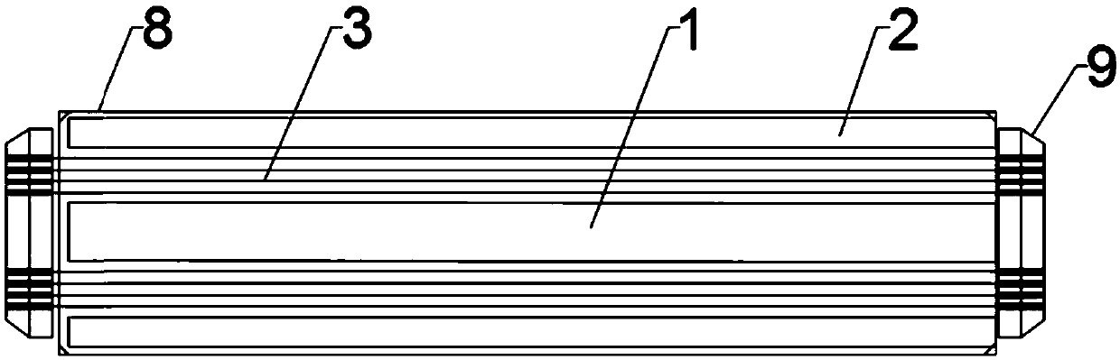
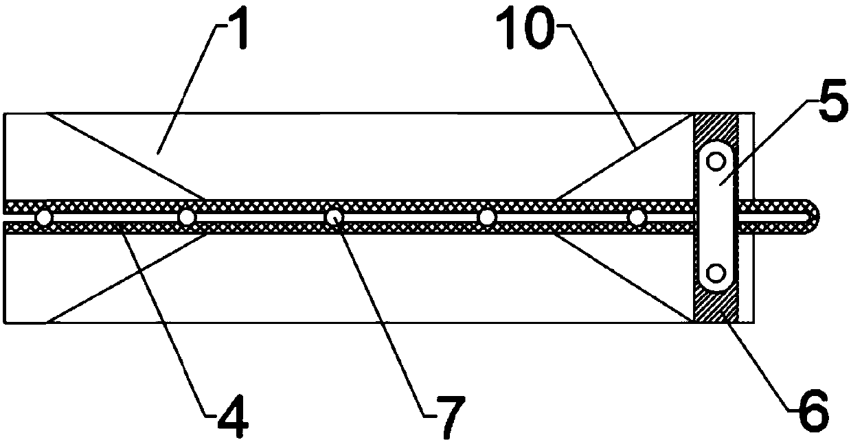
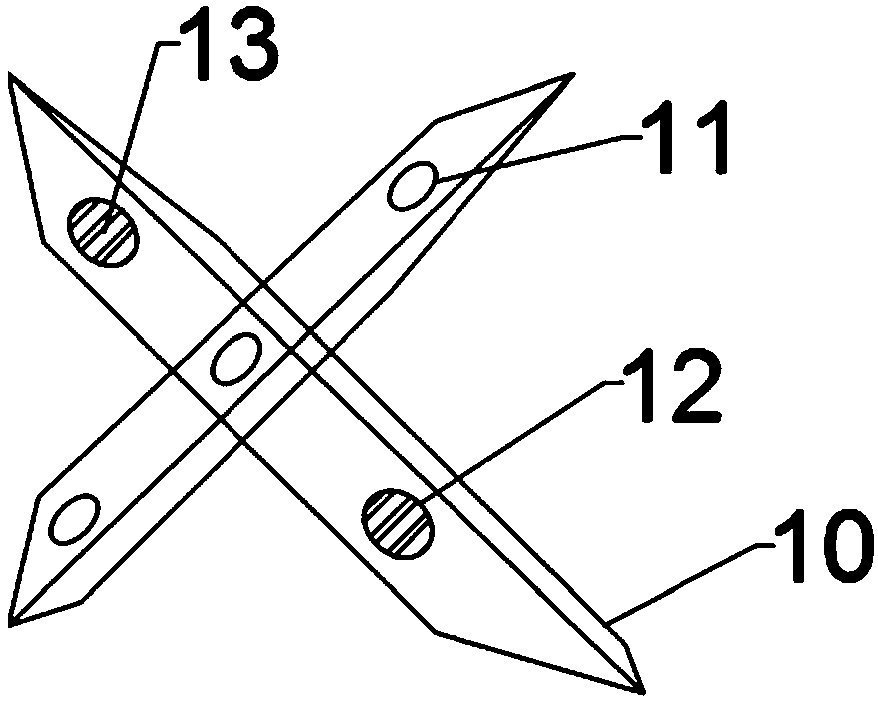
[0040] like Figure 1 to Figure 5 As shown, the present invention provides a flexible printed circuit board, including a flexible substrate 1, and a thermoplastic resin insulating layer 2 is provided on both surfaces of the flexible substrate 1, and the flexible substrate 1 and the thermoplastic resin insulating layer 2 are There are signal line groups 3 parallel to each other therebetween, and the signal line groups 3 are all fixed b...


PUM


Abstract

The invention discloses a method for manufacturing a flexible printed circuit board and provides a manufacturing method. The method comprises the following steps: drilling holes in a soft substrate according to pentagonal star distribution to form a plurality of via holes, exposing a pattern on an original image to a photosensitive base plate, executing development, etching the surface of a singlepanel, arranging a signal line group, respectively arranging multi-port connecting ends at two ends, bending the circuit board at a thermoplastic temperature, executing rapid cooling and shaping, andpressing a connecting surface; the space stability is very good, a three-dimensional multilayer circuit board structure can be conveniently formed, folding, rotation and shaping are directly carriedout, batch production can be achieved by using the same template for many times, the process is simplified, and the production efficiency is improved.

Description

technical field [0001] The invention relates to the technical field of circuit boards, in particular to a manufacturing method of a flexible printed circuit board. Background technique [0002] Flexible printed circuit boards have the characteristics of thin thickness, light weight, dense lines, bendability and flexibility, and are widely used in the field of electronic devices. Flexible printed circuit boards have been widely used to provide wiring for movable parts of electronic devices. In addition, with the reduction in size of electronic devices and the improvement in functions of electronic devices, flexible printed circuit boards by connecting several flexible printed circuit boards together have been used. Flexible printed circuit boards In some specific applications, at least two flexible printed circuit boards can even be soldered into an integrated flexible printed circuit board. [0003] Obviously, the thickness of the soldering position of the integrated flexi...

Claims


Application Information

Patent Timeline
Patent Type & Authority Applications(China)
IPC IPC(8): H05K3/00H05K3/06
CPCH05K1/028H05K3/0014H05K3/0047H05K3/06H05K2203/0278H05K2203/1105
Inventor 方志彦
Owner 邑升顺电子(深圳)有限公司
Why Eureka
Try Eureka