Method for laser polishing of surface of silicon wafer

A silicon wafer surface and laser polishing technology, which is applied in laser welding equipment, electrical components, circuits, etc., can solve the problems of complicated process and cumbersome process, and achieve the effect of simple process, good repeatability and high flexibility

Active Publication Date: 2019-04-30
BEIHANG UNIV +1
View PDF11 Cites 9 Cited by
  • Summary
  • Abstract
  • Description
  • Claims
  • Application Information

AI Technical Summary

Problems solved by technology

The above-mentioned polishing process technology i

Method used


Image

  • Method for laser polishing of surface of silicon wafer
  • Method for laser polishing of surface of silicon wafer
  • Method for laser polishing of surface of silicon wafer

Examples


Embodiment Construction

[0020] In order to better understand the content of the present invention, the technical solution of the present invention will be described in detail below in conjunction with the accompanying drawings and specific embodiments. The examples given are only used to explain the present invention and are not intended to limit the scope of the present invention.

[0021] A method for laser polishing a silicon wafer surface, comprising the steps of:

[0022] Step 1, put the silicon wafer to be treated into deionized water for ultrasonic cleaning, and dry the surface of the cleaned silicon wafer with cold air to obtain a silicon wafer sample with a clean surface;

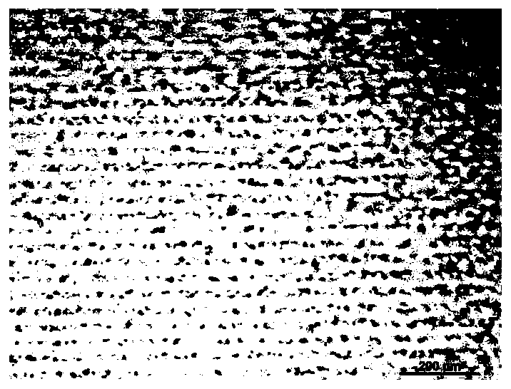
[0023] Step 2: Fix the clean silicon wafer sample obtained in Step 1 on the laser processing platform, set the laser scanning process path and laser processing parameters, and use the laser processing system to scan and process the surface of the silicon wafer;

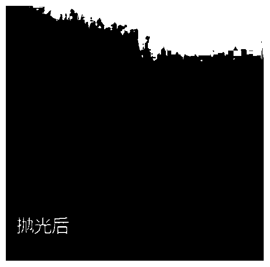
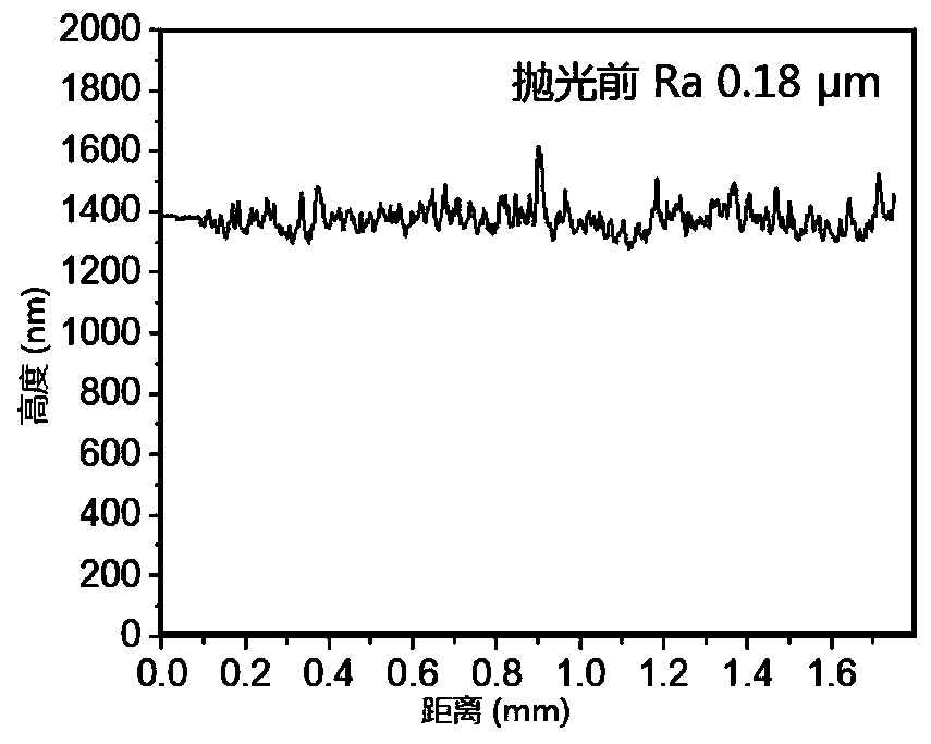
[0024] Step 3: Put the laser-treated silicon wafer sample o...


PUM

PropertyMeasurementUnit
Wavelengthaaaaaaaaaa
Pulse widthaaaaaaaaaa

Abstract

The invention relates to a method for laser polishing of the surface of a silicon wafer, and belongs to the technical field of surface polishing of semiconductor materials. The method comprises the steps that firstly, the silicon wafer is ultrasonically cleaned and blow-dried by cold air; then the surface of the silicon wafer is subjected to scanning processing through a set laser scanning processpath and laser processing parameters by utilizing a laser surface polishing technology; and after processing is completed, ultrasonic cleaning and cold air blow-drying are conducted, and thus the high-precision laser-polished surface is obtained. The preparation method is simple in process, high in efficiency, flexible and controllable, and has great repeatability, and industrialization application is easy to realize.

Description

technical field [0001] The invention relates to a method for laser polishing the surface of a silicon chip, belonging to the technical field of semiconductor material surface polishing. Background technique [0002] Integrated circuit (IC) is the core of the electronic information industry, and electronic information products based on semiconductor integrated circuits have become the world's largest pillar industry. Commonly used semiconductor materials are hard and brittle, and are prone to brittle cracks and cracks during processing. Chemical mechanical polishing (CMP) is currently recognized and widely used in the ultra-precision processing of integrated circuit chips to obtain a smooth and smooth surface. This method combines mechanical friction and chemical corrosion, and has both advantages, and can obtain higher Quality polished finish. However, a large amount of polishing liquid is used in the chemical mechanical polishing process. During the polishing process, the...

Claims


Application Information

Patent Timeline
IPC IPC(8): B23K26/352B23K26/60B23K26/70B23K101/40H01L21/02
CPCB23K26/60B23K26/70H01L21/02008H01L21/02013
Inventor 管迎春张震王海鹏方志浩
Owner BEIHANG UNIV
Why Eureka
Try Eureka