Supercharge Your Innovation With Domain-Expert AI Agents!

Mode-spot converter and making method thereof

A mode spot converter and converter technology, applied in the field of integrated photonics, can solve problems such as increasing process complexity and increasing processing cost, and achieves the effects of being compatible with CMOS technology, low processing and manufacturing cost, and low insertion loss

Active Publication Date: 2019-04-30
ZHONGXING PHOTONICS TECH CO LTD +1
View PDF13 Cites 0 Cited by
  • Summary
  • Abstract
  • Description
  • Claims
  • Application Information

AI Technical Summary

Problems solved by technology

However, this method needs to introduce additional process steps in the original silicon waveguide process, thus increasing the complexity of the process and increasing the processing cost

Method used


Image

  • Mode-spot converter and making method thereof
  • Mode-spot converter and making method thereof
  • Mode-spot converter and making method thereof

Examples


Embodiment 1

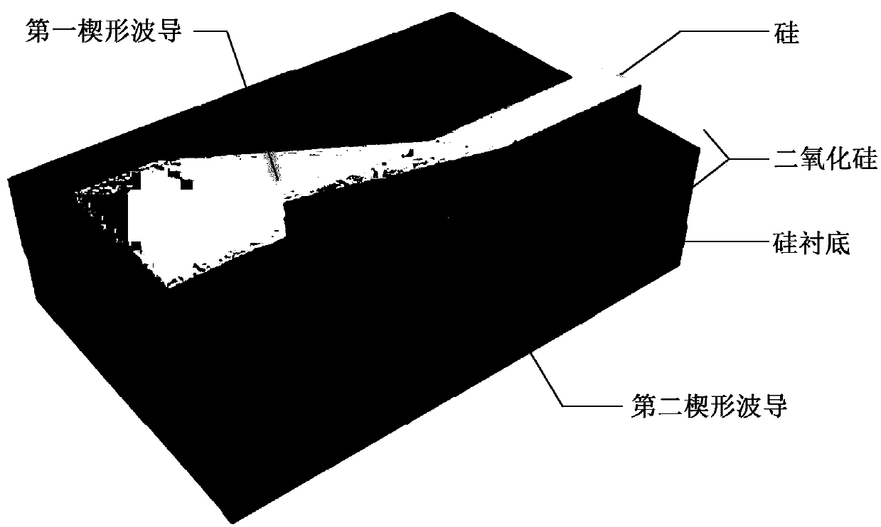
[0056] The thickness of the waveguide layer of the 220nm wafer of the SOI process platform applied to the speckle converter in the embodiment of the present invention is 220nm. The lower cladding material is silicon dioxide with a thickness of 2 μm, and the upper cladding material is silicon dioxide with a thickness of 2˜3 μm.

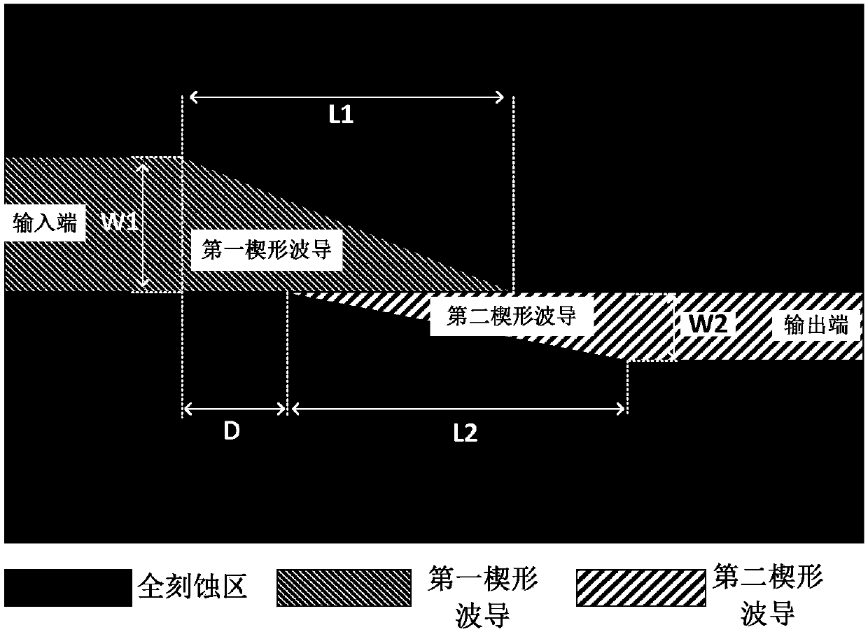
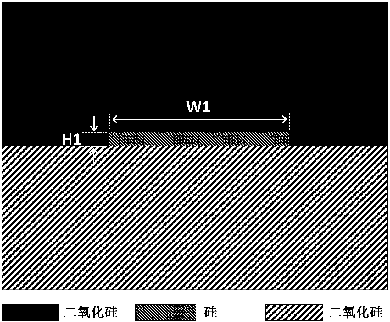
[0057] For the speckle converter shown in Figure 1, the corresponding parameters in this embodiment are: the thickness of the first wedge-shaped waveguide is 70nm, which can be processed by using 150nm deep ridge etching technology to process the silicon waveguide layer with a thickness of 220nm. The width of the input end of the first wedge-shaped waveguide is 4.0 μm. The overall length of the first wedge-shaped waveguide is 20 μm. The thickness of the second wedge-shaped waveguide is 220nm, which is consistent with the thickness of the silicon strip waveguide on the waveguide platform. The width of the output end of the second wedge-shaped waveguid...

Embodiment 2

[0063] The embodiment of the present invention adopts a 310nm wafer on an SOI process platform, and the thickness of its waveguide layer is 300nm. The lower cladding material is silicon dioxide with a thickness of 0.8 μm. The upper cladding material is silicon dioxide, and its thickness is 2-3 μm. For the speckle converter shown in Figure 1, the corresponding parameters in this embodiment are: the thickness of the first wedge-shaped waveguide is 65nm, which can be formed by processing a silicon waveguide layer with a thickness of 300nm by using 235nm deep ridge etching technology . The width of the input end of the first wedge-shaped waveguide is 4.0 μm. The overall length of the first wedge-shaped waveguide is 20 μm. The thickness of the second wedge-shaped waveguide is 300 nm, which is consistent with the thickness of the silicon strip waveguide on the waveguide platform. The width of the output end of the second wedge-shaped waveguide is 0.45 μm. The overall length of ...


PUM


Abstract

Disclosed in the invention are a mode-spot converter and a making method thereof. The mode-spot converter comprises a first wedge waveguide and a second wedge waveguide that are in a reversed butt joint manner. The first wedge waveguide having a wedge structure serves as an input waveguide and is used for realizing end surface coupling with a semiconductor laser or a semiconductor gain chip; and the second wedge waveguide having a wedge structure serves as an output terminal of the second wedge waveguide and is used for coupling with a silicon waveguide. According to the application, the converter can be used for coupling between the semiconductor laser or semiconductor gain chip and the silicon waveguide on an insulating substrate. The structure is simple; the process requirement is low;and the compatibility with the CMOS process is high.

Description

technical field [0001] The invention relates to the field of integrated photonics, in particular to a speckle converter and a manufacturing method thereof. Background technique [0002] In recent years, silicon-based photonic integration technology compatible with complementary metal oxide semiconductor (CMOS, Complementary Metal Oxide Semiconductor) technology has received extensive attention and research from academia and industry. Due to the advantages of high integration and low processing cost, this technology is considered to be the most promising for large-scale photonic integration. At the same time, core devices such as modulators, detectors, attenuators, beam splitters, and filters on the silicon photonics platform are becoming more and more mature, so it is expected to break through the existing communication bandwidth bottleneck and promote communication technology to continue to move toward larger bandwidth and more High-speed, lower-cost progress. However, si...

Claims


Application Information

Patent Timeline
Patent Type & Authority Applications(China)
IPC IPC(8): G02B6/14G02B6/136
CPCG02B6/136G02B6/14
Inventor 陈明华李渔华锋张琦王会涛
Owner ZHONGXING PHOTONICS TECH CO LTD
Features
  • R&D
  • Intellectual Property
  • Life Sciences
  • Materials
  • Tech Scout
  • Unparalleled Data Quality
  • Higher Quality Content
  • 60% Fewer Hallucinations
Learn More