Ohmic contact electrode, HEMT device and preparation method

A technology of ohmic contact electrode and ohmic contact, which is applied in semiconductor/solid-state device manufacturing, electrical components, semiconductor devices, etc., can solve problems such as difficult to use semiconductor ohmic contact, improve electrical parameters and work reliability, and improve ohmic contact Uniformity, the effect of lowering the forming temperature

Inactive Publication Date: 2019-05-03
ZHANGJIAGANG EVER POWER SEMICON
View PDF7 Cites 4 Cited by
  • Summary
  • Abstract
  • Description
  • Claims
  • Application Information

AI Technical Summary

Problems solved by technology

However, wide bandgap semiconductors such as AlGaN and GaN will undergo self-compensation, and it is difficult to obtain ohmic contacts by heavily doping the semiconductor surface.

Method used


Image

  • Ohmic contact electrode, HEMT device and preparation method
  • Ohmic contact electrode, HEMT device and preparation method
  • Ohmic contact electrode, HEMT device and preparation method

Examples


Embodiment Construction

[0026] The following will clearly and completely describe the technical solutions in the embodiments of the present invention with reference to the accompanying drawings in the embodiments of the present invention. Obviously, the described embodiments are only some, not all, embodiments of the present invention. Based on the embodiments of the present invention, all other embodiments obtained by persons of ordinary skill in the art without making creative efforts belong to the protection scope of the present invention.

[0027] The invention provides a kind of preparation method of ohmic contact electrode, it comprises the steps:

[0028] S1. Using photolithography to define the source-drain ohmic contact window.

[0029] S2. Etching the ohmic contact region of AlGaN to a certain thickness. Preferably, the AlGaN ohmic contact region is etched to a thickness of 15-20 nm.

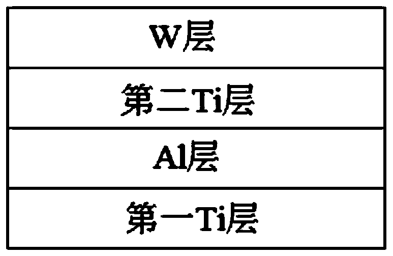
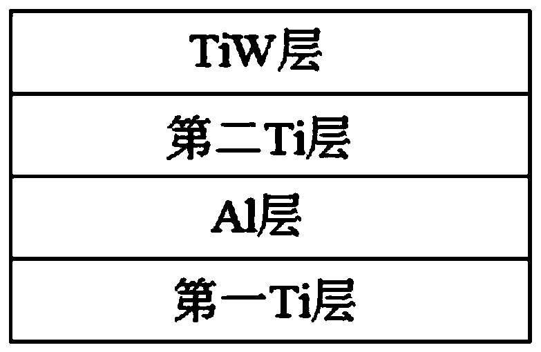
[0030] S3, sequentially depositing metal layers in the source and drain regions. Preferably, the metal ...


PUM

PropertyMeasurementUnit
thicknessaaaaaaaaaa
thicknessaaaaaaaaaa
thicknessaaaaaaaaaa

Abstract

The invention provides an ohmic contact electrode, an HEMT device and a preparation method, and the preparation method comprises the following steps: S1, defining a source-drain ohmic contact window by photoetching; S2, etching an ohmic contact area of AlGaN to a certain thickness; S3, sequentially depositing metal layers in the source-drain region; S4, carrying out alloy annealing treatment by adopting a microwave radiation process after degumming and stripping to form the ohmic contact electrode provided by the invention. According to the preparation method of the ohmic contact electrode, the deposited metal layer is processed in a microwave annealing mode, the formation temperature of the GaN ohmic contact resistor can be reduced, the ohmic contact uniformity is improved, and the electrical parameters and the working reliability of a GaN power device are improved.

Description

technical field [0001] The invention relates to the technical field of semiconductors, in particular to an ohmic contact electrode, a HEMT device and a preparation method. Background technique [0002] Ohmic contact technology is one of the key technologies to realize high-performance GaN HEMT devices. The method of ohmic contact preparation, the morphology and performance of the material directly affect the total conductance, total transconductance, total output power, microwave noise characteristics of the device and the reliability of the device under high power. Selecting appropriate metal materials and realizing heavy doping on the surface of semiconductor materials are common methods to obtain good ohmic contacts in practical processes. Ohmic contacts generally choose metal materials with good electrical conductivity and thermal stability, and a work function close to that of semiconductors, so as to reduce the barrier height between materials. The semiconductor mate...

Claims


Application Information

Patent Timeline
Patent Type & Authority Applications(China)
IPC IPC(8): H01L21/28H01L29/45H01L21/335H01L29/417H01L29/778
Inventor 周炳陈雨雁龙飞陈明光郑国源莫淑一
Owner ZHANGJIAGANG EVER POWER SEMICON
Why Eureka
Try Eureka