A manufacturing process of a P-band low-noise amplifier

A technology of low-noise amplifier and manufacturing process, applied in amplifiers, improved amplifiers to reduce noise impact, amplifiers with semiconductor devices/discharge tubes, etc., can solve the problem that the production and manufacturing process does not have mature technical solutions, affect technology promotion and application, etc. problems, to achieve the effect of scientific manufacturing process, high gain, and high product qualification rate

Pending Publication Date: 2019-05-03
HUADONG PHOTOELECTRIC TECHN INST OF ANHUI PROVINCE
View PDF3 Cites 1 Cited by
  • Summary
  • Abstract
  • Description
  • Claims
  • Application Information

AI Technical Summary

Problems solved by technology

[0004] However, as far as the existing technology is concerned, because the product has not been available for a long time, its manufacturing process does not have a mature technical solution, thus affecting the popularization and application of this technology

Method used


Image

  • A manufacturing process of a P-band low-noise amplifier
  • A manufacturing process of a P-band low-noise amplifier
  • A manufacturing process of a P-band low-noise amplifier

Examples


Embodiment Construction

[0026] The specific implementation of the present invention will be further described in detail by describing the embodiments below with reference to the accompanying drawings, so as to help those skilled in the art have a more complete, accurate and in-depth understanding of the inventive concepts and technical solutions of the present invention.

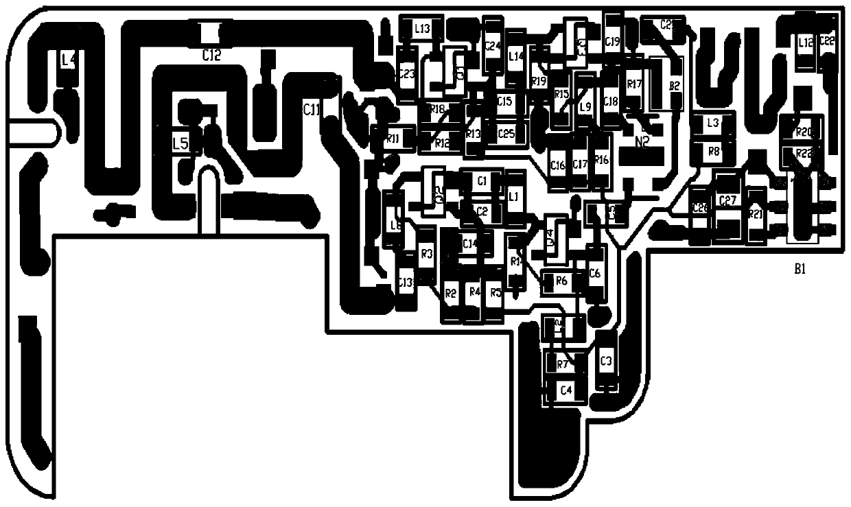
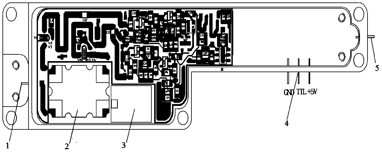
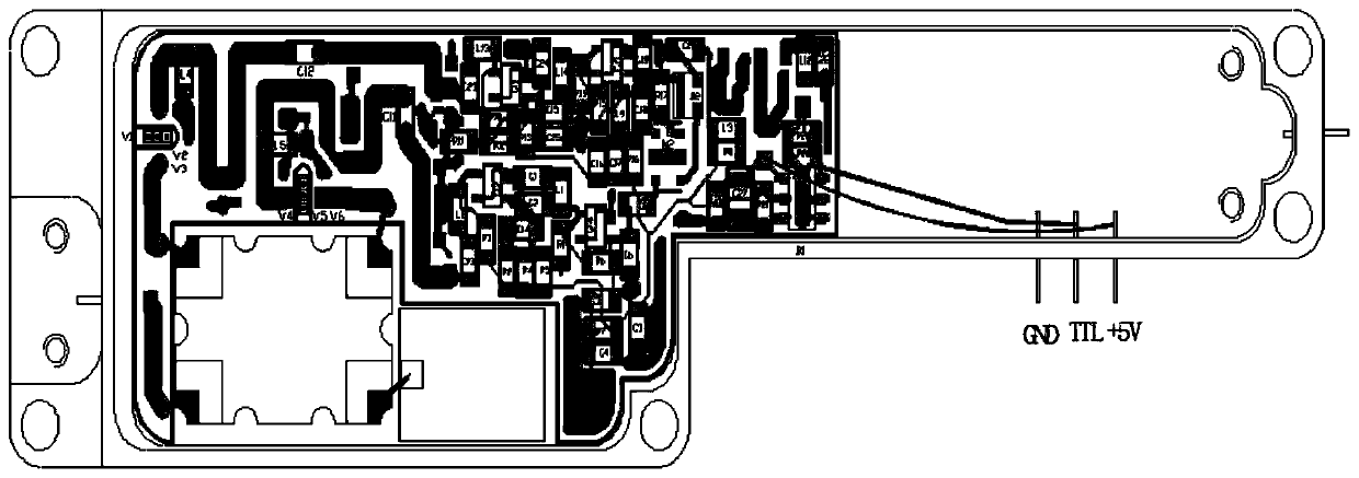
[0027] like figure 1 The structure of the present invention shown is a P-band low noise amplifier. The present invention is the manufacturing process of the P-band low-noise amplifier. In order to realize the invention purpose of the manufacturing process of P wave band low noise amplifier, the technical scheme that the present invention takes is:

[0028] like Figure 1 to Figure 6 As shown, the process of the manufacturing process mainly includes:

[0029] Step 1. Sinter the components onto the circuit board:

[0030] 1.1. Turn on the dispensing machine and adopt the continuous dispensing mode. The pressure of the dispensing ...


PUM

PropertyMeasurementUnit
lengthaaaaaaaaaa

Abstract

The invention discloses a manufacturing process of a P-band low-noise amplifier. The manufacturing process comprises the following steps: 1, sintering a component on a circuit board; 2, sintering theinsulator and the circuit board with the surface-mounted component on the shell; 3, sintering the filter on the shell; 4, gluing the chip; 5, carrying out gold wire bonding at corresponding positions;And 6, performing debugging, testing, capping and marking. By adopting the technical scheme, the P-band low-noise amplifier is high in output power, high in gain, low in noise, wide in frequency bandand high in performance; The P-band low-noise amplifier manufactured and produced through the method is tested, subjected to environment experiments and subjected to complete machine field debugging,and all performance indexes completely meet the requirements of the complete machine; The manufacturing technological process is scientific, simple and convenient, the percent of pass of produced products is high, and the method is suitable for batch production.

Description

technical field [0001] The invention belongs to the technical field of microwave electronic device manufacturing technology. More specifically, the present invention relates to a manufacturing process of a P-band low noise amplifier. Background technique [0002] In a wireless communication system, a Low Noise Amplifier (LNA) is often placed at the forefront of the receiver, its main function is to linearly amplify the weak signal received from the antenna, while suppressing various clutter and noise Interference increases system sensitivity. It is used in electronic systems such as radar, communication, electronic countermeasures, telemetry and remote control, etc., and has very high utilization value. [0003] The P-band low-noise amplifier refers to a power amplifier with an operating frequency in the range of 0.23 to 1 GHz. The P-band low-noise amplifier can be widely used in the radars of the air force, navy and other equipment, and can also be widely used in various...

Claims


Application Information

Patent Timeline
Patent Type & Authority Applications(China)
IPC IPC(8): H03F1/26H03F3/213
Inventor 奚凤鸣周宗明李金晶汪宁聂庆燕俞畅
Owner HUADONG PHOTOELECTRIC TECHN INST OF ANHUI PROVINCE
Why Eureka
Try Eureka