ldmos transistor and method of making the same

A manufacturing method and transistor technology, applied in semiconductor/solid-state device manufacturing, semiconductor devices, electrical components, etc., to achieve the effects of improving carrier mobility, eliminating adverse effects, and reducing short-channel effects

Active Publication Date: 2021-11-26
SEMICON MFG INT (SHANGHAI) CORP +1
View PDF0 Cites 0 Cited by
  • Summary
  • Abstract
  • Description
  • Claims
  • Application Information

AI Technical Summary

Problems solved by technology

The larger breakdown voltage and larger driving current make LDMOS transistors have better switching characteristics and stronger driving capabilities, but it is difficult for existing LDMOS transistors to meet the above two conditions at the same time

Method used


Image

  • ldmos transistor and method of making the same
  • ldmos transistor and method of making the same
  • ldmos transistor and method of making the same

Examples


Embodiment Construction

[0048] A method for manufacturing an LDMOS transistor, comprising the steps of:

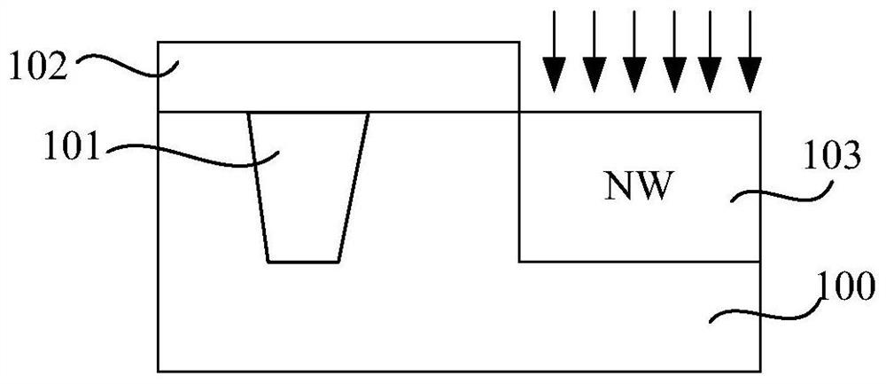
[0049] First, please refer to Figure 1A , providing a P-type semiconductor substrate 100 with a shallow trench isolation (Shallow trench isolation, STI) 101, forming a first patterned photoresist layer 102 on the surface of the semiconductor substrate 100 to expose the Ion-implanted semiconductor substrate surface regions;

[0050] Then, please continue to refer to Figure 1A , using the first patterned photoresist layer 102 as a mask, using N-type ions to perform well ion implantation on the exposed semiconductor substrate surface region, thereby forming an N well (NWELL, NW) 103;

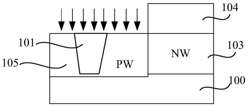
[0051] Next, please refer to Figure 1B , remove the first patterned photoresist layer 102, and form a second patterned photoresist layer 104 on the surface of the semiconductor substrate surface 100, the second patterned photoresist layer 104 covers the N well 103 And expose part of the surface area of ​​the se...


PUM


Abstract

The present invention provides an LDMOS transistor and a manufacturing method thereof. A well region is formed in a first region of a semiconductor substrate, and after the gate stack structure is formed, only ion implantation is performed on the first region of the semiconductor substrate to form at least A doped layer located in the well region, the doping type of the doped layer is opposite to that of the well region, thereby forming an asymmetric ion implantation structure on both sides of the gate stack structure, on the one hand It can increase the channel stress, improve the carrier mobility, and then increase the drive current and breakdown voltage of the device. On the other hand, it can inhibit the diffusion of dopant ions in the source region closer to the gate stack structure to the gate. In the channel region at the bottom of the stack structure, it helps to form a shallower junction, thereby reducing short channel effects and reverse short channel effects, and improving device performance.

Description

technical field [0001] The invention relates to the technical field of integrated circuit manufacturing, in particular to an LDMOS transistor and a manufacturing method thereof. Background technique [0002] Lateral Diffused Metal Oxide Semiconductor (LDMOS) transistors have obvious advantages in terms of key device characteristics such as gain, linearity, and heat dissipation performance, and are also compatible with complementary metal oxide semiconductor (CMOS) processes. , so it has been widely used. Drive current (Ion) and breakdown voltage BV (Breakdown Voltage) are two important parameters to measure the performance of LDMOS devices. Among them, the driving current refers to the current from the drain to the source when the device is working; and the breakdown voltage refers to the highest instantaneous limit voltage value of the designated terminal before the device is broken down. The larger breakdown voltage and larger driving current make the LDMOS transistor ha...

Claims


Application Information

Patent Timeline
Patent Type & Authority Patents(China)
IPC IPC(8): H01L21/336H01L29/06H01L29/78
Inventor 赵猛
Owner SEMICON MFG INT (SHANGHAI) CORP
Why Eureka
Try Eureka