
Metal bonding pad structure and process method thereof

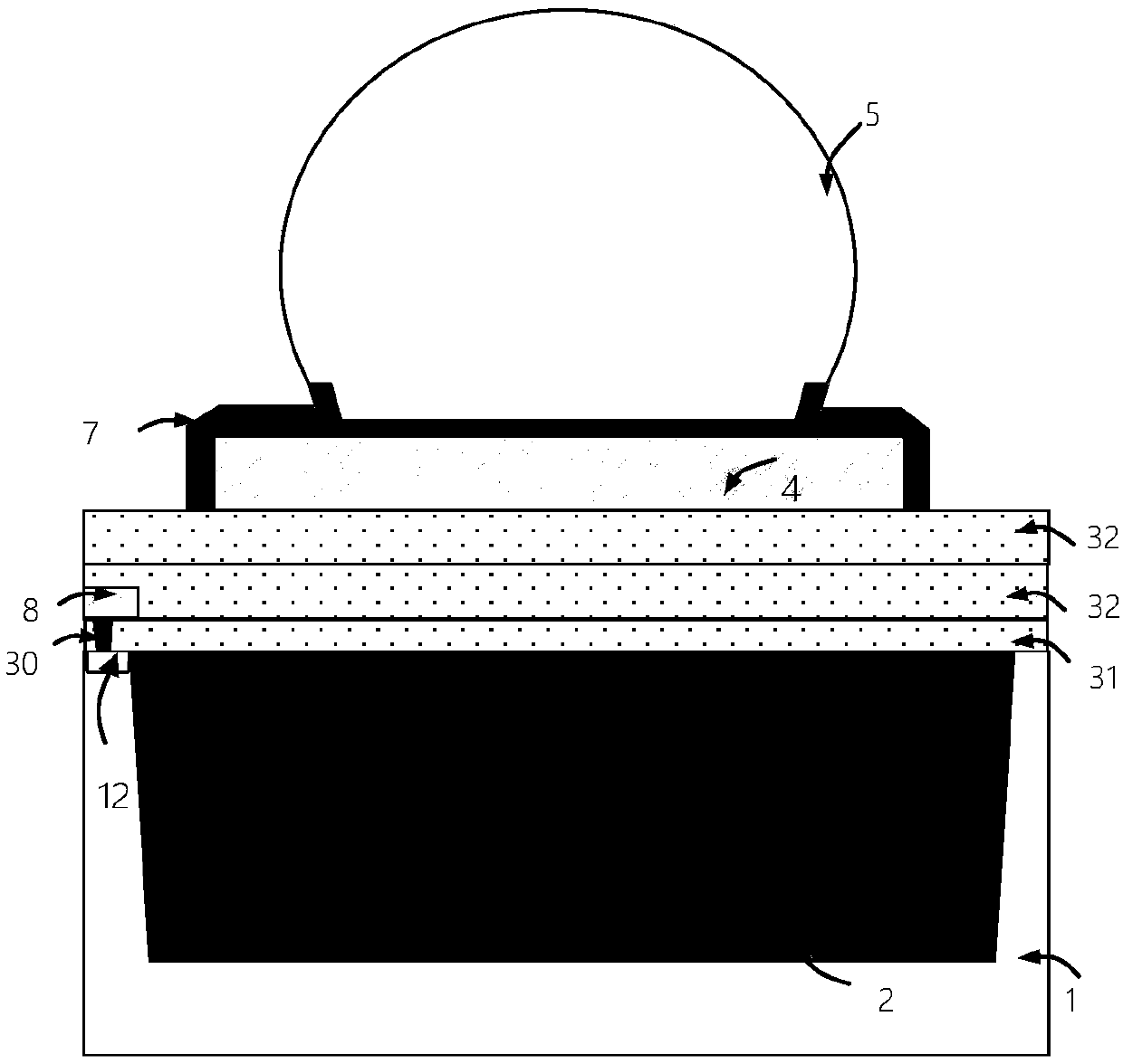
A technology of metal pads and process methods, applied in the direction of electrical components, electric solid devices, circuits, etc., can solve the problems of process cost increase, signal attenuation, increase chip cost, etc., to solve the problem of excessive parasitic capacitance, eliminate parasitic capacitance, Effect of increasing media thickness

Active Publication Date: 2019-05-14
DIOO MICROCIRCUITS CO LTD
View PDF4 Cites 0 Cited by
  • Summary
  • Abstract
  • Description
  • Claims
  • Application Information

AI Technical Summary

Problems solved by technology

[0003] However, chip-level packaging will also bring a problem to high-speed ICs, that is, chip-level packaging mostly adopts ball planting, and the diameter of solder balls is generally 180um and above, which requires the length and width of the chip pad metal to be 200um (microns), the area of ​​such a pad PAD is much larger (4 to 10 times) than that of ordinary wire-bonded packages, which introduces a much larger parasitic capacitance than ordinary packages to the substrate, which may reach several Hundreds of fF, and for the input signal of high-speed IC, that is, the signal with frequency between 800M and 10G, the input capacitance of hundreds of fF will bring considerable signal attenuation. For example, for high-speed switching IC, the transmission of high-speed signal There are two pressure pads that will pass through from the input end to the output end, then the sum of the parasitic capacitance of the pressure pads may reach close to 1pf, which will become the main factor of signal attenuation
[0004] The existing method to reduce parasitic capacitance is to increase the number of chip interconnection metal layers, for example, three layers of metal become five layers, so that the thickness of the medium between the topmost pad metal layer and the grounded silicon substrate is increased, which can realize Capacitance is reduced, but this brings a great increase in process cost. For each additional layer of metal, two process mask levels are added.
This can drastically increase the cost of the chip

Method used


Image

  • Metal bonding pad structure and process method thereof
  • Metal bonding pad structure and process method thereof

Examples


Embodiment Construction

[0032] The implementation of the present invention is described below through specific specific examples, and those skilled in the art can easily understand other advantages and effects of the present invention from the content disclosed in this specification.

[0033] It should be noted that the structures, proportions, sizes, etc. shown in the drawings attached to this specification are only used to match the content disclosed in the specification for the understanding and reading of those familiar with this technology, and are not used to limit the implementation of the present invention Therefore, it has no technical substantive meaning. Any modification of structure, change of proportional relationship or adjustment of size shall fall within the scope of the present invention without affecting the effect and purpose of the present invention. The disclosed technical content must be within the scope covered. At the same time, terms such as "upper", "inner", "outer", "bottom...


PUM


Abstract

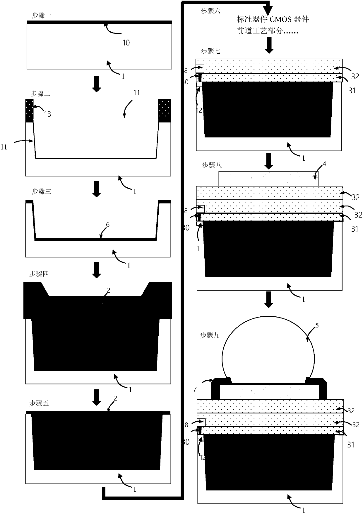
A metal bonding pad structure comprises a substrate, a filling medium, a metal front dielectric layer, a top metal layer and a bonding sphere, wherein a groove is formed in a surface of the substrate,the filling medium is arranged in the groove, the metal front dielectric layer is arranged on the filling medium and the substrate, the top metal layer is arranged on the metal front dielectric layer, and the welding sphere is arranged on the top metal layer. The process method comprises the steps of firstly, thermally growing an initial oxide layer on the surface of the substrate; secondly, photoetching and etching to form the groove, thermally growing a transition layer and depositing the filling medium on the surface of the silicon substrate and a side wall and the bottom of the groove, depositing a multi-layer dielectric layer and the metal layer on the substrate and the filling medium, photoetching a contact hole in the dielectric layer, filling metal, and depositing the top metal layer and a passivation layer for photoetching and etching; and finally, forming lead-tin welding sphere on the top metal layer.

Description

technical field [0001] The invention belongs to the field of manufacturing technology of semiconductor integrated circuits, in particular to a metal pad structure capable of reducing the parasitic capacitance of a pressure pad of a chip package in a high-speed integrated circuit and a process method thereof. Background technique [0002] High-speed integrated circuit (IC) is a type of integrated circuit widely used in mobile portable devices, such as mobile processor interface, super high-speed USB 3.0 switch, etc., in order to meet the small size, thin and light, and stable data transmission of various portable products High-speed ICs generally use wafer-level chip-scale packaging (WLCSP) to meet the application requirements of performance, heat dissipation, etc., and the packaged size is basically the same as the chip size. [0003] However, chip-level packaging will also bring a problem to high-speed ICs, that is, chip-level packaging mostly adopts ball planting, and the ...

Claims


Application Information

Patent Timeline
Patent Type & Authority Applications(China)
IPC IPC(8): H01L23/488H01L21/60
CPCH01L2224/11
Inventor 吕宇强
Owner DIOO MICROCIRCUITS CO LTD
Learn More