

Polycrystalline silicon film deposition method
A technology of polysilicon film and deposition method, applied in gaseous chemical plating, coating, electrical components, etc., can solve the problems of product quality impact, sweeping out, particle defects, etc., to reduce particle defects and improve uniformity.
- Summary
- Abstract
- Description
- Claims
- Application Information
AI Technical Summary
Problems solved by technology
Method used
Image

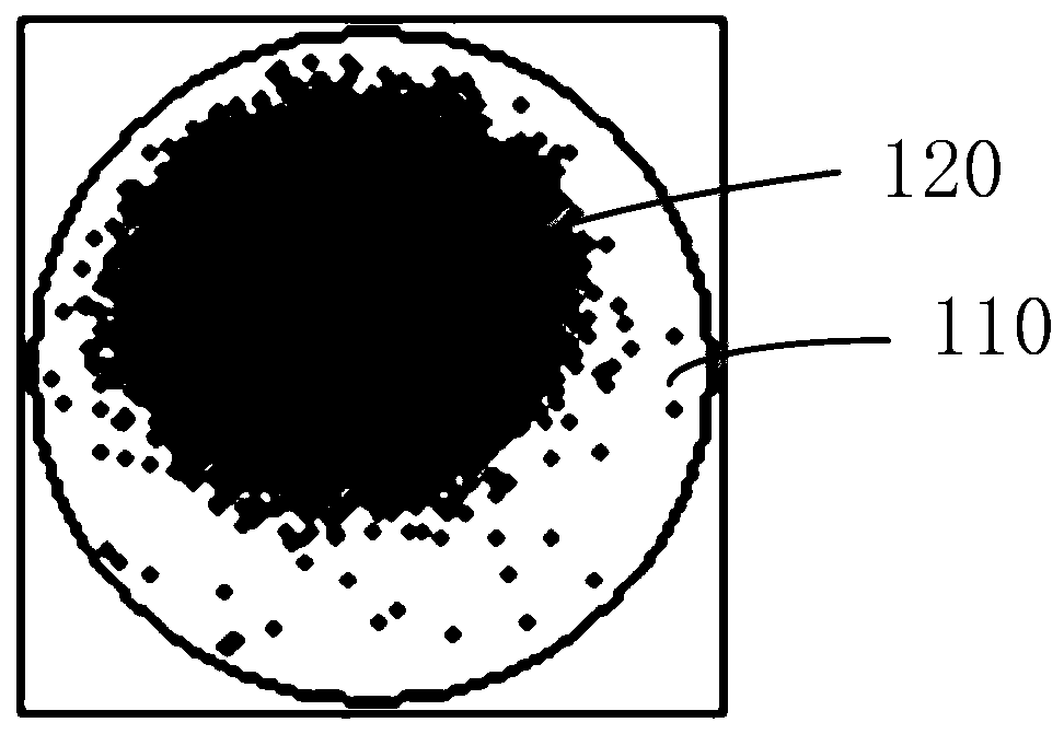
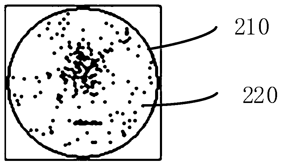
Examples
Embodiment Construction
[0025] The specific implementation manner of the present invention will be described in more detail below with reference to schematic diagrams. Advantages and features of the present invention will be apparent from the following description and claims. It should be noted that all the drawings are in a very simplified form and use imprecise scales, and are only used to facilitate and clearly assist the purpose of illustrating the embodiments of the present invention.
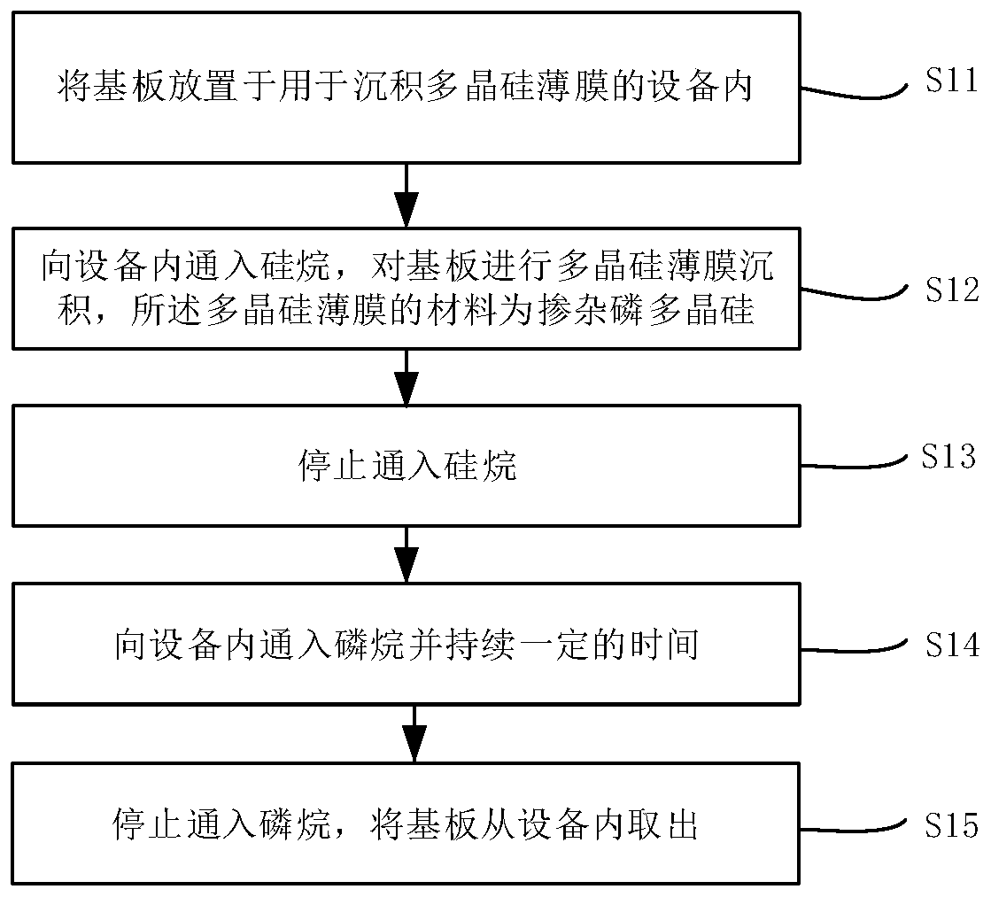
[0026] refer to figure 1 , the invention provides a method for depositing a polysilicon film, comprising:
[0027] S11: placing the substrate in equipment for depositing polysilicon thin films;
[0028] S12: Passing silane into the equipment, and depositing a polysilicon film on the substrate, the material of the polysilicon film is phosphorus-doped polysilicon;
[0029] S13: stop feeding silane;
[0030] S14: Passing phosphine into the equipment for a certain period of time;
[0031] S15: stop feeding phosp...
PUM
 Abstract
Description
Claims
Application Information