

MEMS making method of chip-grade atomic clock vapor cell
A chip-level atomic clock and atomic gas chamber technology, applied in the field of atomic clocks, can solve problems affecting the yield of atomic gas chambers, CPT resonance frequency drift, and differences in alkaline atom content, etc.
- Summary
- Abstract
- Description
- Claims
- Application Information
AI Technical Summary
Problems solved by technology
Method used
Image

Examples
Embodiment Construction
[0030] The present invention will be further described in detail below in conjunction with the accompanying drawings and specific embodiments. It should be noted that all the drawings are in very simplified form and use imprecise ratios, which are only used for the purpose of conveniently and clearly assisting in describing the embodiments of the present invention.
[0031] The specific steps of the MEMS manufacturing method of a chip-level atomic clock atomic gas chamber of the present invention are as follows:
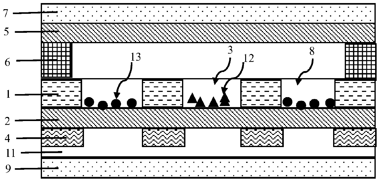
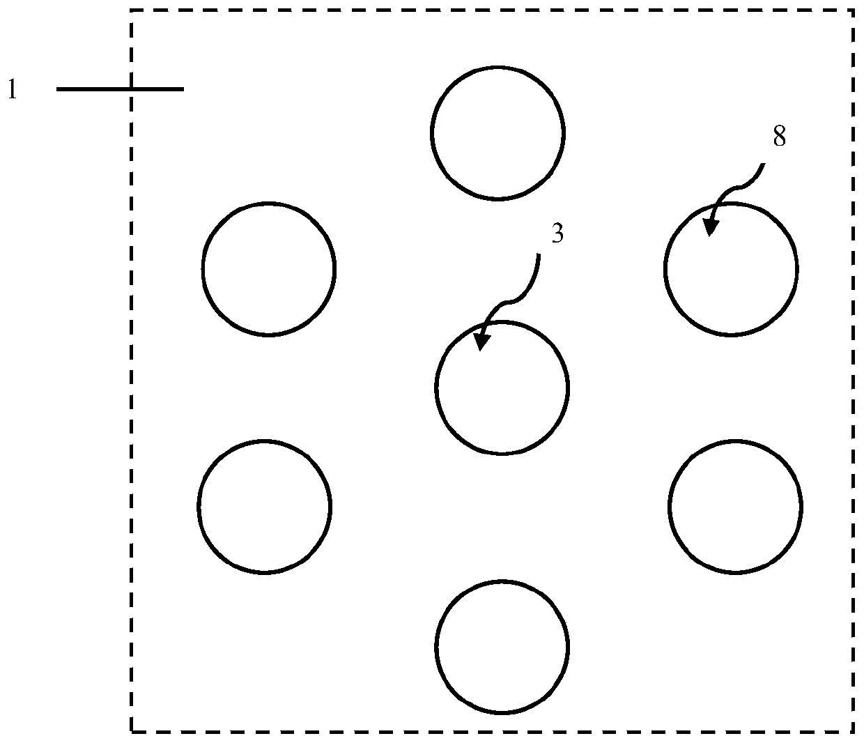
[0032] S1: Carry out laser drilling on the crystalline silicon wafer, clean and polish it to form a silicon wafer (1): refer to the attached figure 2 , is a partial schematic diagram of a perforated silicon wafer in a preferred embodiment of the present invention. On a crystalline silicon wafer with a diameter of about 160 mm, a silicon wafer (1) is obtained by drilling holes with a laser. It is necessary to attach figure 2 It is a partial schematic diagram of a...
PUM
 Abstract
Description
Claims
Application Information