

Low-temperature atomic layer deposition method for oxide film
A technology of atomic layer deposition and oxide thin film, which is applied in the direction of coating, gaseous chemical plating, metal material coating process, etc., can solve the problem of affecting the film properties and device functions, increasing the carbon impurity content of the film, and reducing the dielectric constant of the film and other issues to achieve the effect of expanding the application, improving the quality and increasing the deposition rate
- Summary
- Abstract
- Description
- Claims
- Application Information
AI Technical Summary
Problems solved by technology
Method used
Image

Examples
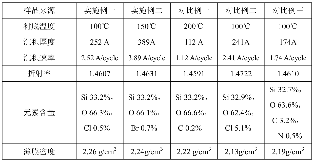
Embodiment 1
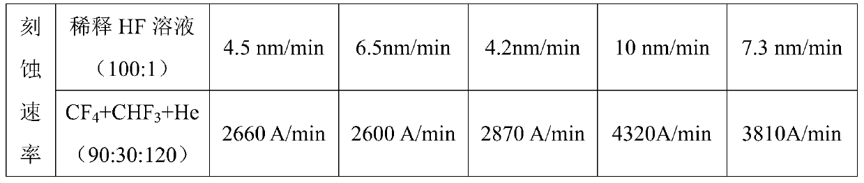
[0036] A SiO 2 Low Temperature Atomic Layer Deposition of Thin Films to SiCl 4 As a precursor material, atomic layer deposition is carried out on the substrate or device. After the chemical adsorption step is completed, the plasma treatment step is used to destroy the Si-Cl bond, effectively remove the halogen residue in the film, and improve the film quality.
[0037] The deposition method includes the following processes:
[0038] (1) Place a 300mm silicon wafer (100) in the ALD cavity and heat it to 100°C, and the SiCl 4 The precursor is introduced into the reaction chamber, and the precursor molecules are chemically adsorbed on the substrate surface;
[0039] (2) After the precursor material forms chemical adsorption on the substrate, extract the excess precursor and purge it with argon (Ar) with a flow rate of 100 sccm and a purge time of 1 sec; continue to feed Ar and light the plasma Body, used to break the chemical bond between Si-Cl, namely: The flow rate is 100s...
Embodiment 2
[0046] A SiO 2 Low temperature atomic layer deposition method of thin films to SiBr 4 As a precursor material, atomic layer deposition is performed on the substrate or device. After the chemical adsorption step is completed, the plasma treatment step is used to destroy the Si-Br bond, effectively remove the halogen residue in the film, and improve the film quality.
[0047] The deposition method includes the following processes:
[0048] (1) Place a 300mm silicon wafer (100) in the ALD chamber and heat it to 150°C; 4 The precursor is introduced into the reaction chamber, and the precursor molecules are chemically adsorbed on the substrate surface;
[0049] (2) After the precursor material forms chemical adsorption on the substrate, extract the excess precursor and purge it with helium (He) with a flow rate of 200 sccm and a purge time of 1 sec; continue to feed He and light the plasma Body, used to break the chemical bond between Si-Br, namely: The He flow rate is 200sccm...
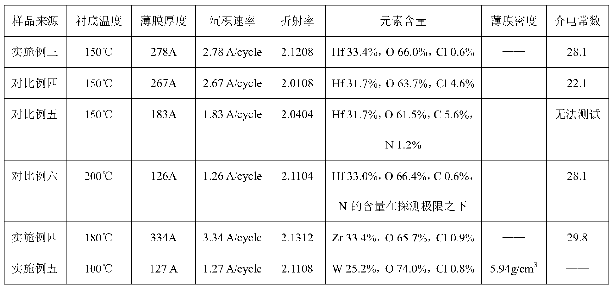
Embodiment 3
[0058] a HfO 2 Low temperature atomic layer deposition method of thin films with HfCl 4 As a precursor material, atomic layer deposition is carried out on the substrate or device. After the chemical adsorption step is completed, the plasma treatment step is used to destroy the Hf-Cl bond, effectively remove the halogen residue in the film, and improve the film quality.
[0059] The deposition method includes the following processes:
[0060] (1) Place a 300mm silicon wafer (100) in an ALD chamber and heat it to 150°C; 4 The stainless steel container is heated to 90°C, and the HfCl is pumped by steam 4 The precursor is introduced into the reaction chamber, and the precursor molecules are chemically adsorbed on the substrate surface;
[0061] (2) After the precursor material forms chemical adsorption on the substrate, extract the excess precursor and purge it with argon (Ar) with a flow rate of 100 sccm and a purge time of 1 sec; continue to feed Ar and light the plasma Body...
PUM
| Property | Measurement | Unit |
|---|---|---|
| density | aaaaa | aaaaa |
| density | aaaaa | aaaaa |
| density | aaaaa | aaaaa |
Abstract
Description
Claims
Application Information