Eureka AIR delivers breakthrough ideas for toughest innovation challenges, trusted by R&D personnel around the world.

Method and system for multi-wavelength laser time-sharing ablation of solar cell dielectric film

A solar cell and dielectric film technology, which is applied in laser welding equipment, circuits, electrical components, etc., can solve the problems of large thermal influence, serious damage, and increased risk of solar cell cracks, so as to improve processing speed, good ablation ability, The effect of improving efficiency and production capacity

Active Publication Date: 2019-05-28
WUHAN DR LASER TECH CORP LTD
View PDF7 Cites 1 Cited by
  • Summary
  • Abstract
  • Description
  • Claims
  • Application Information

AI Technical Summary

Problems solved by technology

Among them, the 808-1064nm laser has a longer wavelength and better penetration, which can take into account both optical absorption and penetration depth, but the heat has a greater impact during processing, and the damage is more serious, which affects the electrical performance of the battery and increases the risk of solar cell cracks; 355nm-532nm laser The processing heat has little impact, but it is easy to be reflected by the passivation layer on the surface of the cell, resulting in energy loss, resulting in incomplete ablation, affecting the subsequent metallization process, and affecting electrical performance

Method used


Image

  • Method and system for multi-wavelength laser time-sharing ablation of solar cell dielectric film
  • Method and system for multi-wavelength laser time-sharing ablation of solar cell dielectric film
  • Method and system for multi-wavelength laser time-sharing ablation of solar cell dielectric film

Examples


Embodiment 1

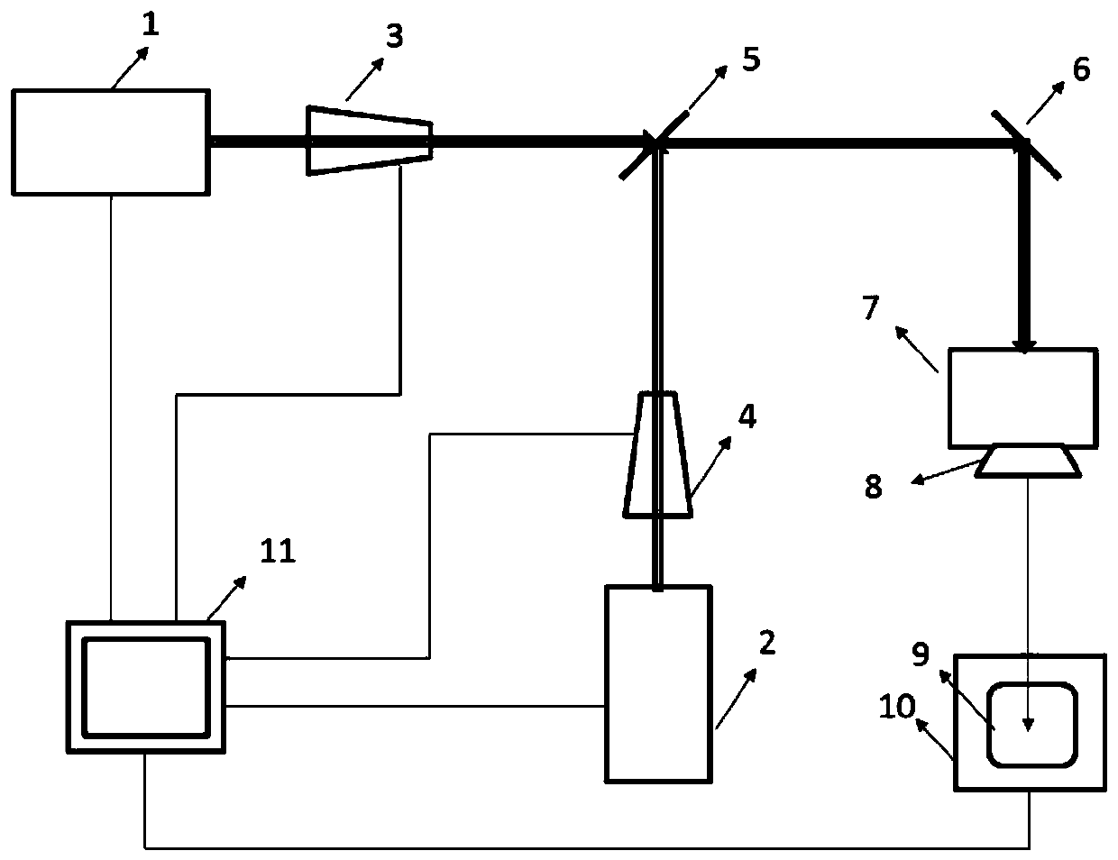
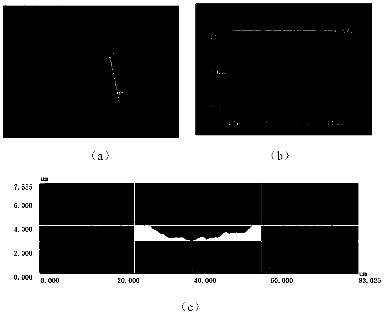
[0043] Embodiment 1 Using the method of the present invention to perform laser ablation on crystalline silicon solar cells, the material of the first layer of the crystalline silicon solar cells in this embodiment is aluminum oxide with a thickness of 10 nm, and the material of the second layer is silicon nitride with a thickness of 150 nm. The wavelength of the first-wavelength laser is 1064nm, the single-point energy is 40μJ, and the spot diameter is 24μm; the wavelength of the second-wavelength laser is 532nm, the single-point energy is 27μJ, and the spot diameter is 33μm. The processing speed is selected as 25m / s, and the time interval between the two lasers is set as 1ns. Facula ablation appearance as Figure 4 As shown, the diameter of the spot is 33 μm, and the depth is 1.51 μm; the comparison shows that the energy of the 1064nm laser is higher than the threshold of the passivation film. Under its synergistic effect, the penetration ability of the 532nm laser is improve...

Embodiment 2

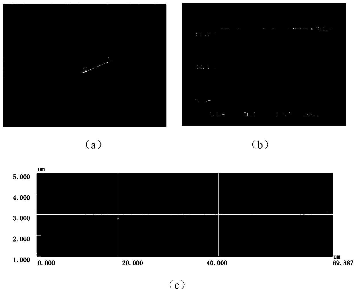
[0044] Embodiment 2 Using the method of the present invention to perform laser ablation on crystalline silicon solar cells, the material of the first layer of the crystalline silicon solar cells in this embodiment is aluminum oxide with a thickness of 10 nm, and the material of the second layer is silicon nitride with a thickness of 150 nm. The wavelength of the first-wavelength laser is 1064nm, the single-point energy is 40μJ, and the spot diameter is 24μm; the wavelength of the second-wavelength laser is 355nm, the single-point energy is 12μJ, and the spot diameter is 38μm. The processing speed is selected to be 25m / s, the time interval between the two lasers is set to 1ns, the final spot diameter is 38μm, and the depth is 0.4μm; the comparison shows that the energy of the 1064nm laser is higher than the threshold of the passivation film. Under its synergy, the 355nm laser The penetration ability is improved, which increases the depth of ablation, which is conducive to improv...

Embodiment 3

[0045] Example 3 Laser ablation of crystalline silicon solar cells is carried out by using the method of the present invention. The material of the first layer of the crystalline silicon solar cells of this embodiment is aluminum oxide with a thickness of 10 nm, and the material of the second layer is silicon nitride with a thickness of 150 nm. The wavelength of the first-wavelength laser is 808nm, the single-point energy is 23μJ, and the spot diameter is 24μm; the wavelength of the second-wavelength laser is 532nm, the single-point energy is 27μJ, and the spot diameter is 33μm. The processing speed is selected as 25m / s, and the time interval between the two lasers is set as 1ns. The final spot diameter is 33 μm, and the depth is 1.45 μm. The comparison shows that the energy of the 808nm laser is higher than the threshold of the passivation film. Under its synergistic effect, the penetration ability of the 532nm laser is improved, which improves the ablation depth, which is con...


PUM

PropertyMeasurementUnit
Wavelength rangeaaaaaaaaaa
Wavelengthaaaaaaaaaa
Thicknessaaaaaaaaaa

Abstract

The invention provides a method and a system for multi-wavelength laser time-sharing ablation of a solar cell dielectric film. The method comprises the steps that at least two coaxial lasers with different wavelengths are adopted, the solar cell dielectric film is sequentially ablated in a time-sharing mode, in one period, each laser emits light one time in turn according to a certain light emitting time interval, and light spots formed by all the lasers in the period are overlapped; the energy density of each laser is higher than the damage threshold value of the corresponding ablation material, and the wavelength of each laser is smaller than the cut-off absorption wavelength of the corresponding ablation material. According to the invention, a multi-wavelength method is adopted, the surface passivation layer of the battery piece is damaged by utilizing the laser with one wavelength, the reflection of the laser to the laser with the next wavelength is reduced, and the ablation capability of the laser with the next wavelength can be better exerted, so that the processing speed is improved, and the efficiency and the productivity are improved under the synergistic effect of the twowavelength lasers.

Description

technical field [0001] The invention belongs to the technical field of photovoltaics, and in particular relates to a method and a system for time-sharing ablation of a solar cell dielectric film by a multi-wavelength laser. Background technique [0002] In the process of high-efficiency crystalline silicon cells, different dielectric layers are often used as passivation films or anti-reflection films to passivate the surface interface states of silicon wafers, reduce surface recombination, and improve cell conversion efficiency. At the same time, the passivation film is often used as a masking layer to block diffusion and form different diffusion regions or metal contact regions. Laser ablation technology is widely used due to its advantages of simplified process, low cost of use, flexible operation, safety and stability. However, for a specific dielectric layer, the ablation effect of a single-wavelength laser is limited. [0003] For example, the back passivation film la...

Claims


Application Information

Patent Timeline
IPC IPC(8): H01L31/18B23K26/36B23K26/362B23K26/073
CPCY02P70/50
Inventor 李志刚马蓉朱凡
Owner WUHAN DR LASER TECH CORP LTD
Why Eureka
Eureka Blog
Learn More