LED epitaxial quantum well growth method

A growth method and quantum well technology are applied in the field of LED epitaxial quantum well growth, which can solve the problems of low luminescence radiation recombination efficiency of quantum wells, and achieve the effects of reducing luminescence attenuation effect, increasing concentration and improving doping efficiency.

Active Publication Date: 2019-06-07
XIANGNENG HUALEI OPTOELECTRONICS
View PDF5 Cites 2 Cited by
  • Summary
  • Abstract
  • Description
  • Claims
  • Application Information

AI Technical Summary

Problems solved by technology

[0004] In view of this, the present invention provides a method for growing LED epitaxial quantum wells, which solves the problem of low recombination efficiency of quantum well luminous radiation existing in existing LED epitaxial growth methods, thereby improving the luminous efficiency of LEDs and reducing warping of epitaxial wafers , improve product yield

Method used


Image

  • LED epitaxial quantum well growth method
  • LED epitaxial quantum well growth method

Examples


Embodiment 1

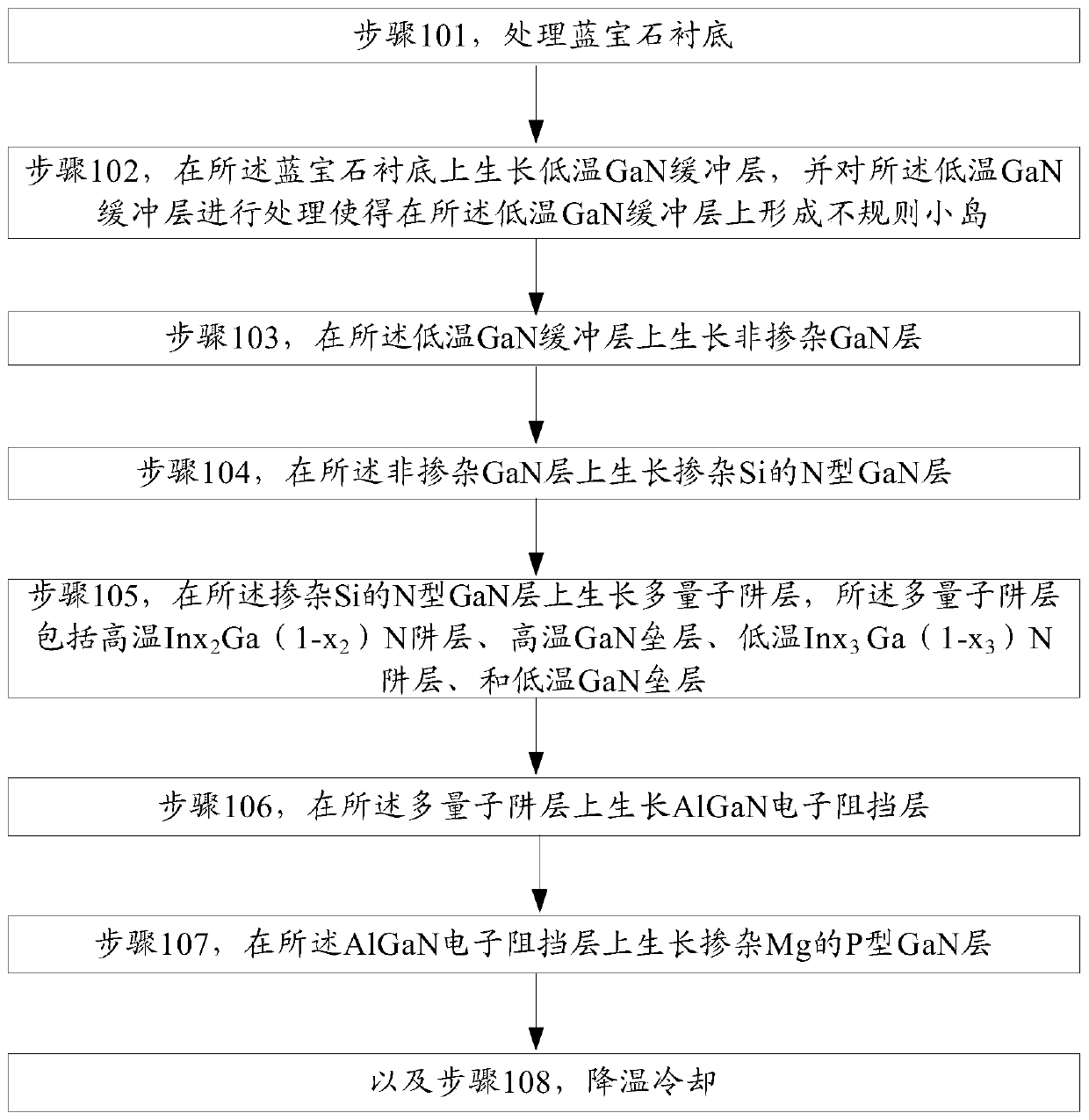
[0050] combine figure 1 , this embodiment provides a LED epitaxial quantum well growth method, the specific steps are as follows:

[0051] Step 101, processing the sapphire substrate:

[0052] At a temperature of 620°C and a reaction chamber pressure of 100mbar, 100L / min of H 2 Conditions, process the sapphire substrate for 5 min.

[0053] Step 102, growing a low-temperature GaN buffer layer on the sapphire substrate, and processing the low-temperature GaN buffer layer to form irregular islands on the low-temperature GaN buffer layer, the specific steps are as follows:

[0054] 1): At a temperature of 500°C and a reaction chamber pressure of 300mbar, 10000sccm of NH is introduced 3 , 50sccm TMGa, 100L / min H 2 Under the condition of , growing the low-temperature GaN buffer layer on the sapphire substrate, the thickness of the low-temperature GaN buffer layer is 20nm;

[0055] 2) At a temperature of 1000°C and a reaction chamber pressure of 300mbar, 30000sccm of NH is intro...

Embodiment 2

[0082] This embodiment also provides a LED epitaxial quantum well growth method, the specific steps are as follows:

[0083] Step 201, processing the sapphire substrate:

[0084] At a temperature of 650°C and a reaction chamber pressure of 300mbar, 130L / min of H 2 Conditions, process the sapphire substrate for 10 min.

[0085] Step 202, growing a low-temperature GaN buffer layer on the sapphire substrate, and processing the low-temperature GaN buffer layer to form irregular islands on the low-temperature GaN buffer layer, the specific steps are as follows:

[0086] 1): At a temperature of 600°C and a reaction chamber pressure of 600mbar, 20000sccm of NH is introduced 3 , 100sccm TMGa, 130L / min H 2 Under the condition of growing the low-temperature GaN buffer layer on the sapphire substrate, the thickness of the low-temperature GaN buffer layer is 40nm;

[0087] 2) At a temperature of 1100°C and a reaction chamber pressure of 600mbar, 40,000 sccm of NH is introduced 3 , 13...

Embodiment 3

[0108] This embodiment also provides a LED epitaxial quantum well growth method, the specific steps are as follows:

[0109] Step 301, processing the sapphire substrate:

[0110] At a temperature of 635°C and a reaction chamber pressure of 200mbar, 120L / min of H 2 conditions, process the sapphire substrate for 7 min.

[0111] Step 302, growing a low-temperature GaN buffer layer on the sapphire substrate, and processing the low-temperature GaN buffer layer to form irregular islands on the low-temperature GaN buffer layer, the specific steps are as follows:

[0112] 1): At a temperature of 550°C and a reaction chamber pressure of 450mbar, 15000 sccm of NH is introduced 3 , 75sccm of TMGa, 115L / min of H 2 Under the condition of growing the low-temperature GaN buffer layer on the sapphire substrate, the thickness of the low-temperature GaN buffer layer is 30nm;

[0113] 2) At a temperature of 1050°C and a pressure of 450mbar in the reaction chamber, 35000 sccm of NH is introdu...


PUM


Abstract

The invention discloses an LED epitaxial quantum well growth method. The method comprises steps: a sapphire substrate is processed; a low-temperature GaN buffer layer grows on the sapphire substrate,the low-temperature GaN buffer layer is processed, and an irregular island is formed on the low-temperature GaN buffer layer; an undoped GaN layer grows on the low-temperature GaN buffer layer; a Si-doped N-type GaN layer grows on the undoped GaN layer; a multi-quantum well layer grows on the Si-doped N-type GaN layer; an AlGaN electron blocking layer grows on the multi-quantum well layer; a Mg-doped P-type GaN layer grows on the AlGaN electron blocking layer; and temperature reduction and cooling are carried out. According to the growth method disclosed in the invention, the light emitting efficiency of the LED can be effectively enhanced, warpage of the epitaxial wafer can be reduced, the qualified rate of the GaN epitaxial wafer is improved, the surface of the epitaxial layer becomes flat, and the appearance is better.

Description

technical field [0001] The invention relates to the technical field of LEDs, and more specifically, to a method for growing LED epitaxial quantum wells. Background technique [0002] A light-emitting diode (Light-Emitting Diode, LED) is a semiconductor electronic device that converts electrical energy into light energy. When current flows, electrons and holes recombine in their quantum wells to emit monochromatic light. As a high-efficiency, environmentally friendly, and green new solid-state lighting source, LED has the advantages of low voltage, low power consumption, small size, light weight, long life, high reliability, and rich colors. At present, the scale of domestic production of LEDs is gradually expanding, but LEDs still have the problem of low luminous efficiency, which affects the energy-saving effect of LEDs. [0003] In the current traditional LED epitaxy InGaN / GaN multi-quantum well layer growth method, the quality of the InGaN / GaN multi-quantum well layer i...

Claims


Application Information

Patent Timeline
Patent Type & Authority Applications(China)
IPC IPC(8): H01L33/00H01L33/06H01L33/12H01L33/14H01L33/32
Inventor 徐平季辉何鹏
Owner XIANGNENG HUALEI OPTOELECTRONICS
Why Eureka
Try Eureka