Post-processing method for obtaining large-grain high-quality perovskite thin film and application thereof

A post-processing, perovskite technology, applied in semiconductor devices, electrical components, photovoltaic power generation, etc., can solve the problems of perovskite film surface morphology changes, prone to pinholes, small particle size, etc., and achieve oxidation time The effect of shortening, reducing the impact of device performance, and low cost

Active Publication Date: 2019-06-07
湖州市鹑火光电有限公司
View PDF3 Cites 11 Cited by
  • Summary
  • Abstract
  • Description
  • Claims
  • Application Information

AI Technical Summary

Problems solved by technology

[0006] Compared with the two-step solution method, the one-step solution method is simpler, but the surface morphology of the perovskite film prepared by the one-step solution method varies greatly, which is often difficult to control, and the particle size is small, and pinholes are prone to appear on the surface, especially for CH 3 NH 3 PB 3 in terms of

Method used


Image

  • Post-processing method for obtaining large-grain high-quality perovskite thin film and application thereof
  • Post-processing method for obtaining large-grain high-quality perovskite thin film and application thereof
  • Post-processing method for obtaining large-grain high-quality perovskite thin film and application thereof

Examples


Embodiment 1

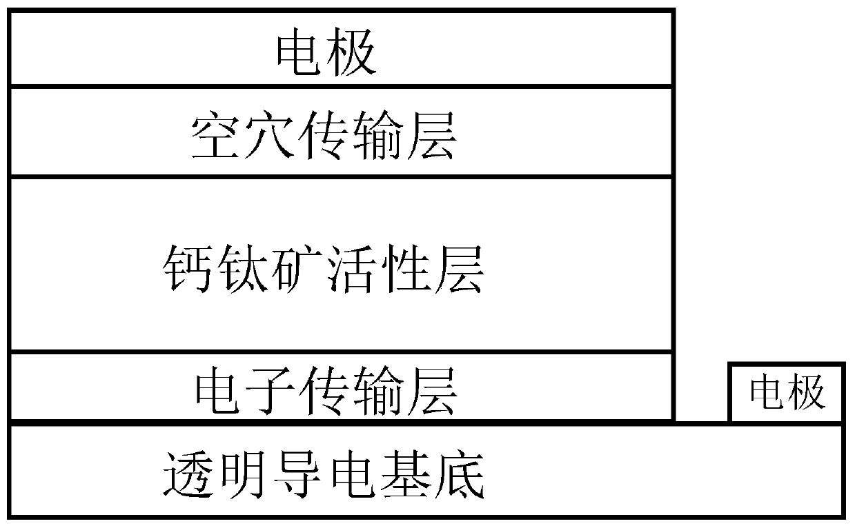
[0041] The battery structure of this implementation example is as figure 1 As shown, it includes five parts: substrate, electron transport layer, perovskite layer, hole transport layer and back electrode. The thickness of the perovskite layer is about 360nm, and the hole transport layer is about 150nm. The specific preparation process is as follows:

[0042] (1) Cleaning and processing the substrate. Use detergent, deionized water, ethanol, acetone, isopropanol, and ethanol to ultrasonically clean for 15 minutes, then dry the substrate with nitrogen, and then treat it with UV-ozone for 15 minutes to obtain SnO 2 base.

[0043] (2) Configure and prepare SnO 2 Spin coater. The mass fraction that will be purchased is 20wt% SnO 2 Take an appropriate amount of the aqueous colloid solution in a clean glass bottle, add deionized water at a ratio of 1:7.35 for dilution, and then oscillate ultrasonically for 30 minutes. The well-mixed diluted solution is then filtered through a fi...

Embodiment 2

[0054] The battery structure of this implementation example is as figure 1 As shown, it includes five parts: substrate, electron transport layer, perovskite layer, hole transport layer and back electrode. The thickness of the perovskite layer is about 520nm, and the hole transport layer is about 150nm. The specific preparation process is as follows:

[0055] (1) Cleaning and processing the substrate. Use detergent, deionized water, ethanol, acetone, isopropanol, and ethanol to ultrasonically clean for 15 minutes, then dry the substrate with nitrogen, and then treat it with UV-ozone for 15 minutes to obtain SnO 2 base.

[0056] (2) Configure and prepare SnO 2 Spin coater. The mass fraction that will be purchased is 20wt% SnO 2 Take an appropriate amount of the aqueous colloidal solution in a clean glass bottle, dilute it with deionized water at a ratio of 1:7, and then vibrate ultrasonically for 30 minutes. The well-mixed diluted solution is then filtered through a filter....

Embodiment 3

[0067] The battery structure of this implementation example is as figure 1 As shown, it includes five parts: substrate, electron transport layer, perovskite layer, hole transport layer and back electrode. The thickness of the perovskite layer is about 520nm, and the hole transport layer is about 150nm. The specific preparation process is as follows:

[0068] (1) Cleaning and processing the substrate. Use detergent, deionized water, ethanol, acetone, isopropanol, and ethanol to ultrasonically clean for 15 minutes, then dry the substrate with nitrogen, and then treat it with UV-ozone for 15 minutes to obtain SnO 2 base.

[0069] (2) Configure and prepare SnO 2 Spin coater. The mass fraction that will be purchased is 20wt% SnO 2 Take an appropriate amount of the aqueous colloidal solution in a clean glass bottle, dilute it with deionized water at a ratio of 1:7, and then vibrate ultrasonically for 30 minutes. The well-mixed diluted solution is then filtered through a filter....


PUM

PropertyMeasurementUnit
thicknessaaaaaaaaaa
thicknessaaaaaaaaaa
thicknessaaaaaaaaaa

Abstract

The present invention belongs to the technical field of photoelectric devices, and discloses a post-processing method for obtaining a large-grain high-quality perovskite thin film and an application thereof. A post-processing technology of a perovskite thin film adopts a gradient annealing technology assisted by mixed solvent steam, and comprises a specific process of: first, conducting thermal annealing at a slightly low temperature; then conducting thermal annealing assisted by mixed solvent steam; and finally conducting thermal annealing at a slightly high temperature to prepare a large-grain high-quality perovskite thin film. The perovskite thin film of the present invention has simple preparation technology, low cost, good repeatability and strong practicability, and is suitable for large-area thin films and large-scale batch processing.

Description

technical field [0001] The invention belongs to the technical field of optoelectronic device preparation, and in particular relates to a post-processing method and application thereof for obtaining large-grain high-quality perovskite thin films. Background technique [0002] As an inexhaustible and clean energy source, solar energy is almost not subject to geographical restrictions. Therefore, capturing solar energy and converting it effectively has become an important way to solve human energy problems. Photovoltaic cells can effectively convert solar energy directly into electrical energy without going through other intermediate channels. It is one of the most effective, extensive and important technologies for human beings to utilize solar energy. As a new type of solar cell technology, perovskite solar cells (PSCs) are unmatched by other new types of solar cells in terms of development speed and attention. The rate of increase in the photoelectric conversion efficiency...

Claims


Application Information

Patent Timeline
Patent Type & Authority Applications(China)
IPC IPC(8): H01L51/48H01L51/00H01L51/42
CPCY02E10/549
Inventor 黄跃龙田柳文章文峰于华
Owner 湖州市鹑火光电有限公司
Why Eureka
Try Eureka