
A high-bandwidth high-gain trans-impedance amplifier applied to a large input capacitor

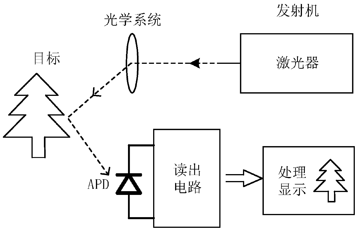
A transimpedance amplifier and capacitor technology, applied in the field of analog signal processing, can solve problems such as bandwidth and gain limitations, and achieve high gain, improved circuit structure, and high bandwidth.

Active Publication Date: 2019-06-07
UNIV OF ELECTRONICS SCI & TECH OF CHINA
View PDF7 Cites 1 Cited by
  • Summary
  • Abstract
  • Description
  • Claims
  • Application Information

AI Technical Summary

Problems solved by technology

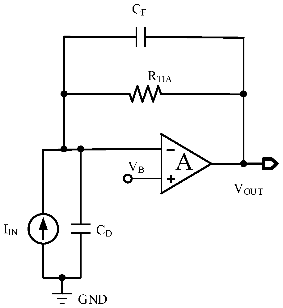
[0003] Aiming at the shortcomings of the above-mentioned traditional transimpedance amplifier when the input capacitance of the avalanche diode with a large photosensitive surface is large, its bandwidth and gain are limited by the input capacitance of the avalanche diode. The present invention proposes a transimpedance amplifier circuit with higher gain and Bandwidth, which solves the problem that the bandwidth and gain of traditional transimpedance amplifiers are limited by the input capacitance of avalanche diodes, and can adapt to large input capacitances, especially for large photosensitive surface avalanche diode array readout circuits

Method used


Image

  • A high-bandwidth high-gain trans-impedance amplifier applied to a large input capacitor
  • A high-bandwidth high-gain trans-impedance amplifier applied to a large input capacitor
  • A high-bandwidth high-gain trans-impedance amplifier applied to a large input capacitor

Examples


Embodiment Construction

[0021] The specific embodiments of the present invention will be described below with reference to the accompanying drawings:

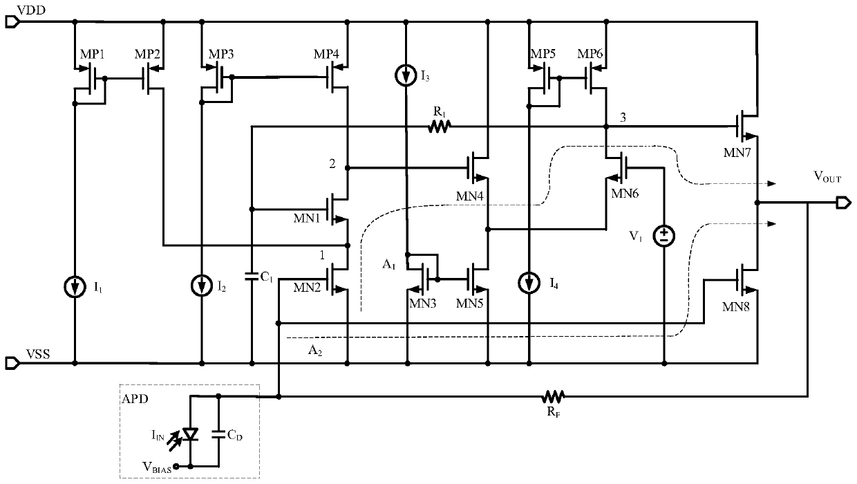
[0022] The specific circuit of the transimpedance amplifier proposed by the present invention is as follows image 3 As shown, including a first NMOS tube MN1, a second NMOS tube MN2, a third NMOS tube MN3, a fourth NMOS tube MN4, a fifth NMOS tube MN5, a sixth NMOS tube MN6, a seventh NMOS tube MN7, and an eighth NMOS tube MN8, first PMOS tube MP1, second PMOS tube MP2, third PMOS tube MP3, fourth PMOS tube MP4, fifth PMOS tube MP5, sixth PMOS tube MP6, first resistor R 1 , The second resistor R F , The first capacitor C 1 , The first current source I 1 , The second current source I 2 , The third current source I 3 , The fourth current source I 4 And bias voltage source V 1 The gate of the second NMOS tube MN2 is connected to the gate of the eighth NMOS tube MN8 and serves as the input end of the transimpedance amplifier, and its drain is connected to the...


PUM


Abstract

The invention discloses a high-bandwidth high-gain trans-impedance amplifier applied to a large input capacitor, and belongs to the field of analog signal processing in laser three-dimensional imaging. The invention can adopt to application conditions of a large input capacitor, and can be especially applied to a large photosensitive surface avalanche diode array read-out circuit. The transimpedance amplifier comprises a slow path and a fast path, the slow path comprises two stages of amplifiers, the first stage of amplifier is a cascode structure formed by a second NMOS transistor and a firstNMOS transistor, the second stage of amplifier is a cascode amplifier formed by a sixth NMOS transistor MN6, and the slow path provides the main gain of the system; The eighth NMOS tube is a common-source amplifier, a fast channel is formed, a feedforward path is provided for the system, and the stability of the system is improved; The fast path and the slow path are connected in parallel in thesystem to generate a left half-plane zero point to replace a compensation capacitor in a traditional transimpedance amplifier, so that the Q value of the system is reduced, the stability of the transimpedance amplifier is realized, and the problem that the bandwidth and the gain of the traditional transimpedance amplifier are limited by the input capacitance of an avalanche diode is solved.

Description

Technical field [0001] The invention belongs to the field of analog signal processing in laser three-dimensional imaging, and relates to a transimpedance amplifier applied to a large input capacitance, and in particular to a type that can be used in a large photosensitive surface avalanche diode (Avalanche Photodiode, APD) array readout circuit A transimpedance amplifier with high gain and high bandwidth. Background technique [0002] Laser 3D imaging technology is a main branch of laser radar technology (Laser Detection and Ranging, LADAR). Compared with traditional 2D remote sensing image technology, laser 3D imaging technology can obtain the 3D information of the target more accurately and is widely used in intelligence. Military and civilian fields such as reconnaissance, unmanned driving, target recognition, precision guidance and safety monitoring. Laser 3D imaging is mainly composed of laser, avalanche diode array and corresponding readout circuit (ReadoutCircuits, ROIC),...

Claims


Application Information

Patent Timeline
Patent Type & Authority Applications(China)
IPC IPC(8): H03F1/48H03F3/68
Inventor 甄少伟章玉飞周万礼曾鹏灏胡怀志罗萍张波
Owner UNIV OF ELECTRONICS SCI & TECH OF CHINA
Learn More