

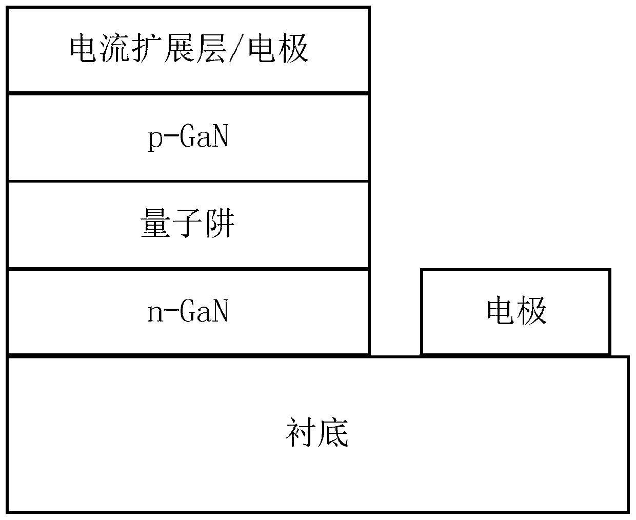
An InGaN-based micron LED photoelectric detector array and application thereof
A technology of photodetectors and LED devices, which is applied in the field of visible light communication and can solve problems such as limiting data rates
- Summary
- Abstract
- Description
- Claims
- Application Information
AI Technical Summary
Problems solved by technology
Method used
Image


Examples
Embodiment 1
[0039] see image 3 , shows a structural diagram of an experimental device for performing single-channel visible light communication using an InGaN micro-LED photodetector array according to a specific embodiment of the present invention.
[0040] The experimental device includes a signal encoding and input unit 1, such as a waveform generator, voice signal, and video signal, used to give a communication signal source; a laser diode 2 as a transmitter, used to send visible light, outside the laser diode and a micron LED photoelectric The detector has a lens series 3 to collimate the emitted light and focus the received light; the light is incident on the micron LED photodetector array 4 for light reception, signal decoding and output unit 5, such as oscilloscope, voice signal and video signal decoding The unit detects the signal received by the micro LED photodetector array 4 .
[0041] In this embodiment, a 405nm laser diode is used as a light transmitter for single-channel ...
Embodiment 2
[0046] see Figure 6 , shows a structural diagram of an experimental device for performing multi-channel (2×2 MIMO) visible light communication using the above-mentioned InGaN micro-LED photoelectric array device according to a specific embodiment of the present invention.
[0047] The experimental setup includes a signal encoding and input unit 1, such as a waveform generator, used to give a parallel communication signal source; a plurality of laser diodes 2, used to transmit visible light; a lens series 3, to collimate and focus the emitted light to a micron LED photoelectric The detector array has 4 receiving ends.
[0048] In this embodiment, two 405nm laser diodes are used as optical transmitters for dual-channel (2×2MIMO) visible light communication; the experiment adopts high-speed parallel communication of on-off keying (OOK) modulation scheme, and the modulated emitted light passes through 1m Free space distance transmission; between each laser diode and the micron L...
Embodiment 3
[0052] see Figure 9 , shows a structural diagram of an experimental device for performing duplex visible light communication using the above-mentioned InGaN micro LED photodetector array according to a specific embodiment of the present invention.
[0053] The experimental setup includes uplink and downlink. Signal encoding and input unit 1, such as a waveform generator, to give the source of the uplink communication signal; laser diode 2, to transmit visible light; lens series 3, to collimate and focus the emitted light to the array of micron LED photodetectors 4 At the receiving end, the signal converted by the micron LED photodetector is decoded and output unit 5 , for example, the signal is displayed and analyzed by an oscilloscope 5 . Downlink, another signal encoding and input unit 1, such as a waveform generator, is used to transmit downlink signals; the micron LED array 6 is used as the transmitting end for transmitting visible light; the lens series 3 collimates and...
PUM
 Abstract
Description
Claims
Application Information