
Eureka
For R&D, Eureka makes reading and utilizing patents & technical documents easy.
Eureka AIR
Designed for self-driven R&D workflows. Generate viable solutions, solve complex R&D challenges, empower your innovation with AI.

Eureka Materials
Designed for material experts only. Revolutionize your material R&D, from search, analyze, to developing new materials.

TechResearch
Generate reliable direction feasibility study reports for your R&D in just a few steps.

TechSeek
Discover and master advanced knowledge NOW. Basics, ideas, possibilities, all at once.

TechMind
As an expert in R&D Theories, TechMind can generates customized viable solutions instantly.

TechRisk
Analyze your overall solution with one click, know your potential R&D risks in advance.

TechMonitor
Get weekly tech updates, stay abreast of the latest tech innovations and key insights.
Photodetection thin film, photodetector and photodetection device
A light detection and thin-film technology, applied in the field of optical devices, can solve problems such as low signal-to-noise ratio and limited application range
- Summary
- Abstract
- Description
- Claims
- Application Information
AI Technical Summary
Problems solved by technology
Method used
Image

Examples
Embodiment 1
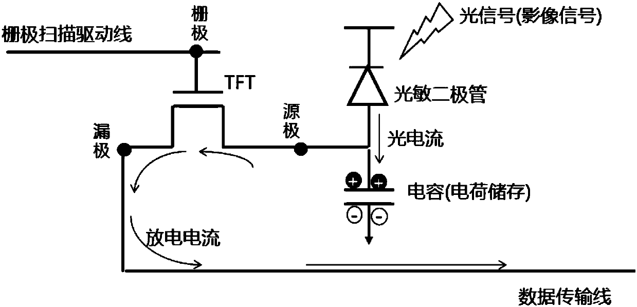
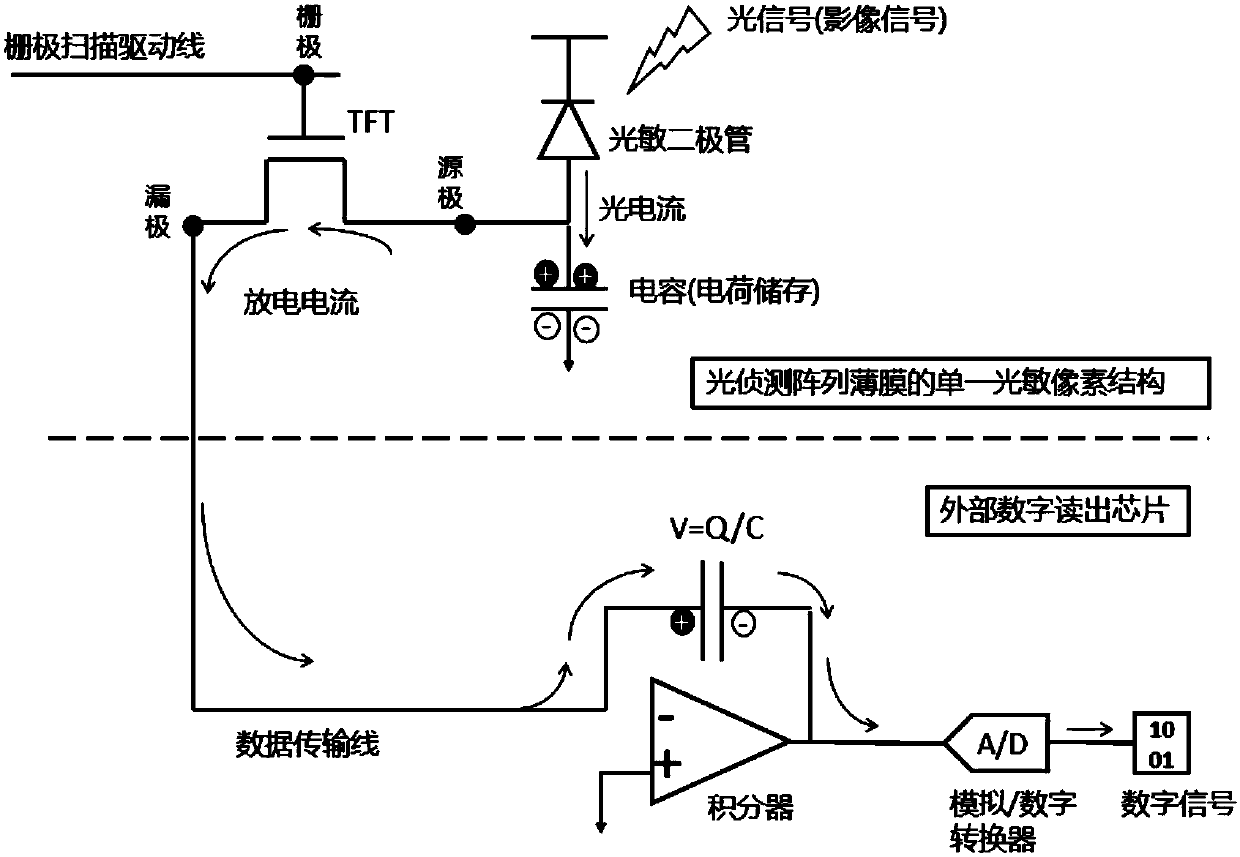
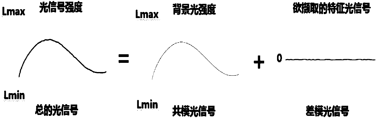
[0067] Such as Figure 4As shown, the photodetection film 501 includes a first gate switch 201 (hereinafter referred to as "TFT11"), a source 2, a drain 3, a first photosensitive diode 202 (hereinafter referred to as "diode 1"), a first capacitor 203 (hereinafter referred to as "capacitor 1"); the first gate switch 201 is arranged between the source 2 and the drain 3, for receiving the first gate scanning drive line 205 (hereinafter referred to as "gate scanning After the first switch turn-on signal transmitted by the driving line 1"), it is in the turn-on state to conduct the source 2 and the drain 3; the first photosensitive diode 202 is used to receive the first photocurrent, and the photocurrent (Here refers to Figure 4 The photocurrent 1 in , representing the photocurrent converted by diode 1) includes the first differential mode current (ie Figure 4 The differential mode current in ) and the first common mode current ( Figure 4 Common mode current 1 in the middle; ...
Embodiment 2
[0079] Such as Figure 7 As shown in FIG. 2 , it is a schematic diagram of the output of the differential mode signal by the photodetection film involved in another embodiment of the present invention. The light detection film includes a first gate switch 201 (ie TFT11), a source, a drain, a first photosensitive diode (ie diode 1), a first capacitor (ie capacitor 1); the first gate switch It is arranged between the source and the drain, and is used for turning on the source and the drain after receiving the first switch start signal transmitted by the first gate scanning driving line, so as to turn on the source and the drain; the first The photodiode is used to receive a first photocurrent, the photocurrent includes a first differential mode current and a first common mode current, the first photodiode is connected to a first capacitor, and the first capacitor is connected to a source;
[0080] The photodetection film also includes a common mode elimination circuit, and the ...
Embodiment 3
[0091] Such as Figure 5 As shown, the difference between the third embodiment and the second embodiment is that the number of the third gate switch is two, including the fourth gate switch 304 (ie TFT21) and the fifth gate switch 305 (ie TFT22), the The third capacitor 303 (i.e. capacitance d) is arranged between the fourth gate switch and the fifth gate switch, the fourth gate switch is arranged between the first photodiode and the third capacitor, and the fifth gate switch Located between the second photosensitive diode and the third capacitor, the fourth gate switch and the fifth gate switch share the second gate scanning driving line.
[0092] see Image 6 In this embodiment, two groups of TFTs are used to scan and drive the two photodiodes with different turn-on times, specifically by inputting a switching signal 1 to the gate scanning driving line 1 and inputting a switching signal 2 to the grid electrode scanning driving line 2 , the two switch signals will open two ...
PUM
 Abstract
Description
Claims
Application Information
 - R&D Engineer
- R&D Manager
- IP Professional
- Industry Leading Data Capabilities
- Powerful AI technology
- Patent DNA Extraction
Browse by: Latest US Patents, China's latest patents, Technical Efficacy Thesaurus, Application Domain, Technology Topic, Popular Technical Reports.
© 2024 PatSnap. All rights reserved.Legal|Privacy policy|Modern Slavery Act Transparency Statement|Sitemap|About US| Contact US: help@patsnap.com