Crosslinking hole transport layer material and preparation method thereof

A technology of hole transport layer and electron transport layer, which is applied in the field of cross-linkable hole transport layer material and its preparation, to achieve the effect of improving performance, improving interface properties, and simple preparation method

Inactive Publication Date: 2019-06-11
SHENZHEN CHINA STAR OPTOELECTRONICS SEMICON DISPLAY TECH CO LTD
View PDF3 Cites 6 Cited by
  • Summary
  • Abstract
  • Description
  • Claims
  • Application Information

AI Technical Summary

Problems solved by technology

[0004] The application provides a cross-linkable hole transport layer material and its preparation method, which can effectively solve the problem of mutual solubility between different functional layers, effectively improve the interface properties of inkjet printing devices, thereby improving the performance of the device

Method used


Image

  • Crosslinking hole transport layer material and preparation method thereof
  • Crosslinking hole transport layer material and preparation method thereof
  • Crosslinking hole transport layer material and preparation method thereof

Examples


Embodiment Construction

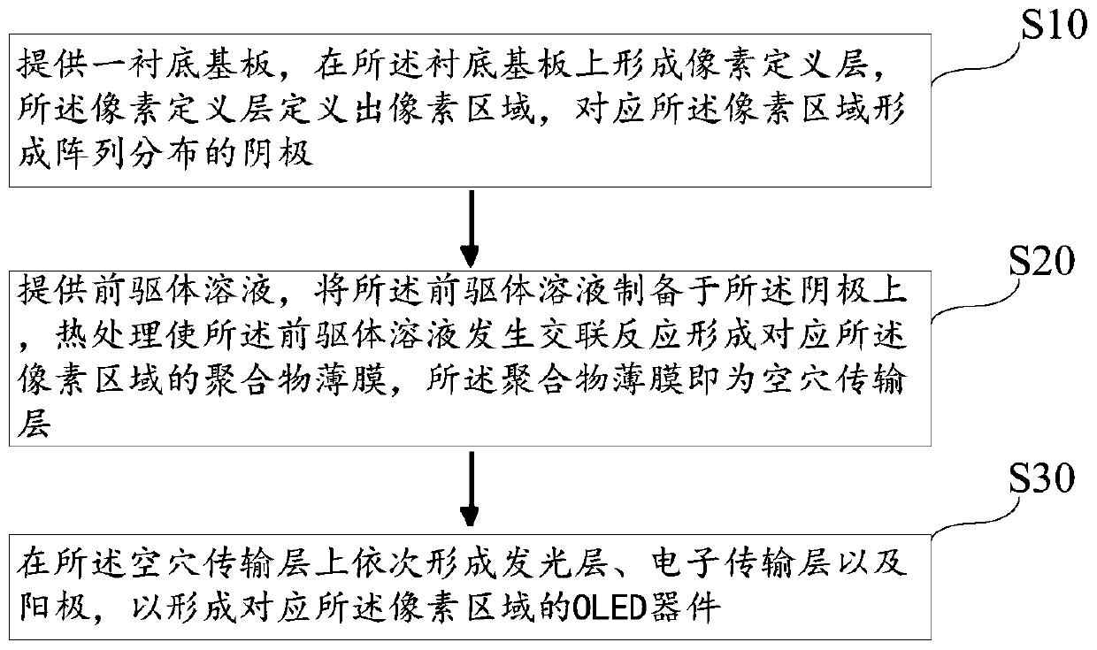
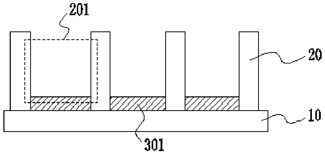
[0028] The following descriptions of the various embodiments refer to the accompanying drawings to illustrate specific embodiments that the present application can be used to implement. The directional terms mentioned in this application, such as [top], [bottom], [front], [back], [left], [right], [inside], [outside], [side], etc., are for reference only The orientation of the attached schema. Therefore, the directional terms used are used to illustrate and understand the application, but not to limit the application. In the figures, structurally similar elements are denoted by the same reference numerals.

[0029] The present application is aimed at the existing OLED display panel, and there is a technical problem of miscibility between materials of different functional layers of the OLED device, and this embodiment can solve this defect.

[0030] The OLED display panel provided by this application includes passive matrix type and active matrix type. In the active matrix OLE...


PUM


Abstract

The invention provides a crosslinking hole transport layer material and a preparation method thereof, and is applied into an OLED display panel. The OLED display panel comprises a substrate and OLED devices manufactured on the substrate at intervals; the OLED devices comprise a cathode, a hole transport layer, a light-emitting layer, an electron transport layer and an anode. The preparation methodof the hole transport layer comprises the following steps: providing a precursor solution comprising precursor molecules and an organic solvent, wherein the precursor molecules are porphyrin molecules or phthalocyanine molecules, and the precursor molecules comprise crosslinking radicals; preparing the pecursor solution onto the cathode, carrying out heat treatment so that a crosslinking reactionoccurs on the precursor solution to form a uniform and stable polymer film, namely the hole transport layer, so that the interfacial property of an ink-jet printing device is improved effectively, and the performance of the device is further promoted.

Description

technical field [0001] The present application relates to the field of display technology, in particular to a crosslinkable hole transport layer material and a preparation method thereof. Background technique [0002] Solution-processed OLED devices, especially ink-jet printed OLED devices, have received more and more attention due to their low cost, no need for metal masks, and high material utilization in the fabrication of large-area panels. It is well known that OLED devices contain multi-layer structures: emissive layer (EML), electron transport layer (ETL), hole transport layer (HTL), etc. Therefore, how to solve the problem of mutual solubility between different functional layers in the preparation process of the device has always been is a big challenge. Using an orthogonal solvent system can alleviate this problem to a certain extent, but most organic materials still have a certain solubility in the upper solvent, which brings great difficulties to the selection of...

Claims


Application Information

Patent Timeline
Patent Type & Authority Applications(China)
IPC IPC(8): H01L51/50H01L51/54H01L51/56
CPCH10K50/00H10K71/00
Inventor 史婷
Owner SHENZHEN CHINA STAR OPTOELECTRONICS SEMICON DISPLAY TECH CO LTD
Why Eureka
Try Eureka