Supercharge Your Innovation With Domain-Expert AI Agents!

Avalanche photodiode

An avalanche photoelectric and diode technology, applied in circuits, electrical components, semiconductor devices, etc., can solve problems such as malfunctioning components, and achieve the effects of increasing the maximum amplified current, improving light sensitivity, and reducing internal resistance

Active Publication Date: 2019-06-14
SHARP KK
View PDF10 Cites 2 Cited by
  • Summary
  • Abstract
  • Description
  • Claims
  • Application Information

AI Technical Summary

Problems solved by technology

This is due to the following problems: assuming that the irradiated light is visible light, there may be malfunctions caused by natural light (visible light) existing in the environment, or there may be concerns about the operation of components due to the irradiated light entering the eyes, etc.
[0007] like Figure 9 As shown schematically, in this SPAD 100, a high electric field is applied to the junction AJ between the N diffusion layer 111 and the p well 112, causing an avalanche phenomenon

Method used


Image

  • Avalanche photodiode
  • Avalanche photodiode
  • Avalanche photodiode

Examples


no. 1 approach

[0049] (Avalanche photodiode configuration)

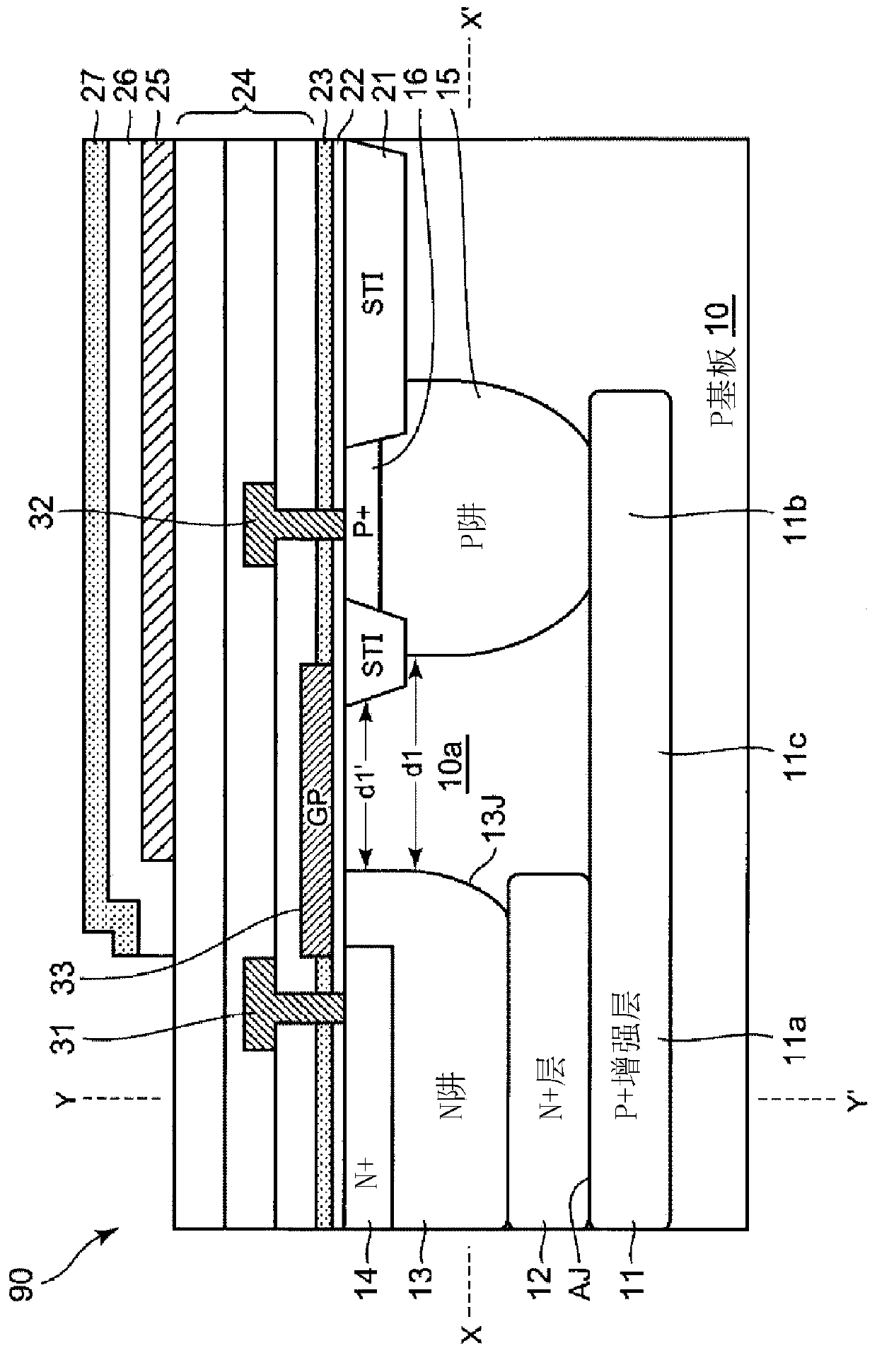
[0050] figure 1 A cross-sectional structure of an avalanche photodiode (SPAD) 90 according to the first embodiment of the present invention is shown. This SPAD 90 includes a P substrate (silicon substrate) 10 having a uniform impurity concentration (resistivity of about 10Ω·cm) as a substrate semiconductor layer. It includes: P+ enhancement layer (impurity concentration 1×10 17 cm -3 left and right) 11, as the first semiconductor layer, formed in the interior of the P substrate 10 (about 2 μm in depth) to occupy a predetermined area in the lateral direction; N+ layer (impurity concentration 2×10 17 cm -3 About), which is used as the second semiconductor layer, which is formed on the P+ enhancement layer in contact with it; N well (about 2 μm in depth, impurity concentration of 3×10 16 cm -3 Left and right) 13, which is used as the third semiconductor layer, formed in contact with the N+ layer 12, and has a lower impurity con...

no. 2 approach

[0074] Figure 6 A cross-sectional structure of an avalanche photodiode (SPAD) 90A according to the second embodiment of the present invention is shown. In addition, in Figure 6 For and figure 1Components in the same components are denoted with the same reference numerals, and repeated descriptions are omitted.

[0075] The SPAD90A, with respect to figure 1 The SPAD 90 differs in that the first portion 11a of the P+ enhancement layer 11A that exists directly below the N+ layer 12 and the second portion 11b that exists directly below the P well 15 are only separated from each other by a distance d2( 2μm or so). Other components of the SPAD90A are with figure 1 The configuration of the SPAD90 is the same.

[0076] In the case of manufacturing this SPAD90A, the implantation mask used in the process of forming the P+ enhancement layer 11A by ion implantation is set to be used for forming figure 1 The implantation mask of the P+ enhancement layer 11 of the SPAD 90 is ch...


PUM

PropertyMeasurementUnit
electrical resistivityaaaaaaaaaa

Abstract

The present invention provides an avalanche photodiode. The avalanche photodiode in a substrate semiconductor layer (10) of a first conductivity type having a uniform impurity concentration comprises:a first semiconductor layer (11) of the first conductivity type; a second semiconductor layer (12) of a second conductivity type; a third semiconductor layer (13) of the second conductivity type; a fourth semiconductor layer (14) of the second conductivity type; a fifth semiconductor layer (15) of the first conductivity type, which is formed at a position apart from the third semiconductor layer(13) in the transverse direction; a sixth semiconductor layer (16) of the second conductivity type; a first contact (31); and a second contact (32). The first semiconductor layer (11) is directly below the second semiconductor layer (12) and the fifth semiconductor layer (15), and is in contact with the second semiconductor layer (12) and the fifth semiconductor layer (15). The avalanche phenomenon is caused at a junction (AJ) between the first semiconductor layer (11) and the second semiconductor layer (12).

Description

[0001] Citation [0002] This application claims the priority rights and interests of Japanese application Japanese Patent Application No. 2016-218553 filed on November 9, 2016, and uses all the content of the Japanese application. technical field [0003] The present invention relates to an avalanche photodiode, and more specifically, to an avalanche photodiode that generates an avalanche phenomenon and operates in a Geiger mode when a reverse bias voltage higher than a breakdown voltage is applied. Background technique [0004] In the fields of optical communication, time of flight (TOF: Time of flight), vehicle-mounted imaging lidar (SPADLIDAR (Single Photon Avalanche Diode Light Detection And Ranging, Single Photon Avalanche Diode Light Detection And Ranging, single photon avalanche diode laser detection and ranging)) and other fields, the use of 850nm , Infrared laser light with a wavelength of 940nm. This is due to the following problems: if the irradiated light is vi...

Claims


Application Information

Patent Timeline
Patent Type & Authority Applications(China)
IPC IPC(8): H01L31/107
CPCH01L31/107H01L29/0642H01L31/02027H01L31/0203H01L31/02363
Inventor 夏秋和弘泷本贵博内田雅代
Owner SHARP KK
Features
  • R&D
  • Intellectual Property
  • Life Sciences
  • Materials
  • Tech Scout
  • Unparalleled Data Quality
  • Higher Quality Content
  • 60% Fewer Hallucinations
Learn More