Plasma etching reactor

A plasma and anti-plasma technology, applied in the direction of discharge tubes, electrical components, circuits, etc., can solve the problems of reducing the service life of equipment, difficult to remove coatings, corrosion chambers, etc., to improve structural stability and improve processing Efficiency, the effect of reducing production costs

Inactive Publication Date: 2019-06-21
ADVANCED MICRO FAB EQUIP INC CHINA
View PDF5 Cites 7 Cited by
  • Summary
  • Abstract
  • Description
  • Claims
  • Application Information

AI Technical Summary

Problems solved by technology

The processing of the prior art will cause the following problems: One problem is that after the etching of a wafer is completed, the inner wall surface of the cavity will be corroded during the process of removing the residual coating, which will reduce the service life of the equipment
The second problem is about the roughness of the inner wall surface of the cavity. When the inner wall surface of the above-mentioned cavity is relatively rough, it is difficult to remove the coating remaining on the inner wall surface of the cavity, so it is still remaining on the surface of the cavity. Coating on the inner wall surface As the number of wafer etching increases, the above-mentioned residual coating will become thicker and thicker, which will eventually affect the stability of plasma etching more quickly or slowly
The third problem is the stability of the chemical composition on the inner wall surface of the cavity. When the plasma used for plasma etching contains F ions, the PSY coated on the inner wall surface of the cavity 2 o 3 The coating will be converted to contain YF 3 Or the coating surface of YOF; the YOF mentioned here is a compound containing three elements of Y, O and F. According to the different chemical components of the plasma, the ratio between the three elements of Y, O and F is also different. different valences), similarly, when the plasma used for plasma etching contains O ions, the inner surface of the cavity is coated with PS YF 3 The coating will be converted into a coating surface containing YOF; then the coating on the inner wall surface of this unstable cavity will also affect the stability of plasma etching

Method used


Image

  • Plasma etching reactor
  • Plasma etching reactor
  • Plasma etching reactor

Examples


Embodiment Construction

[0027] The present invention will be further elaborated below by describing a preferred specific embodiment in detail with reference to the accompanying drawings.

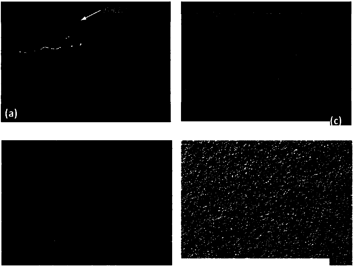
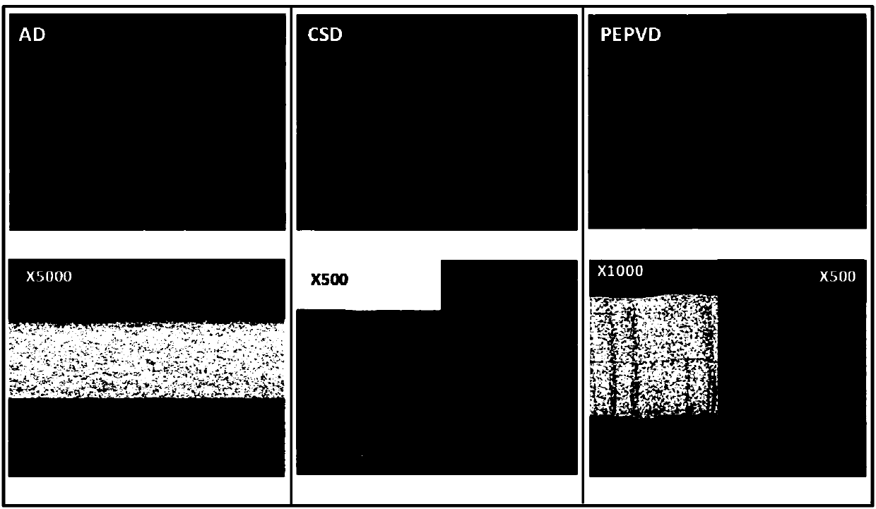
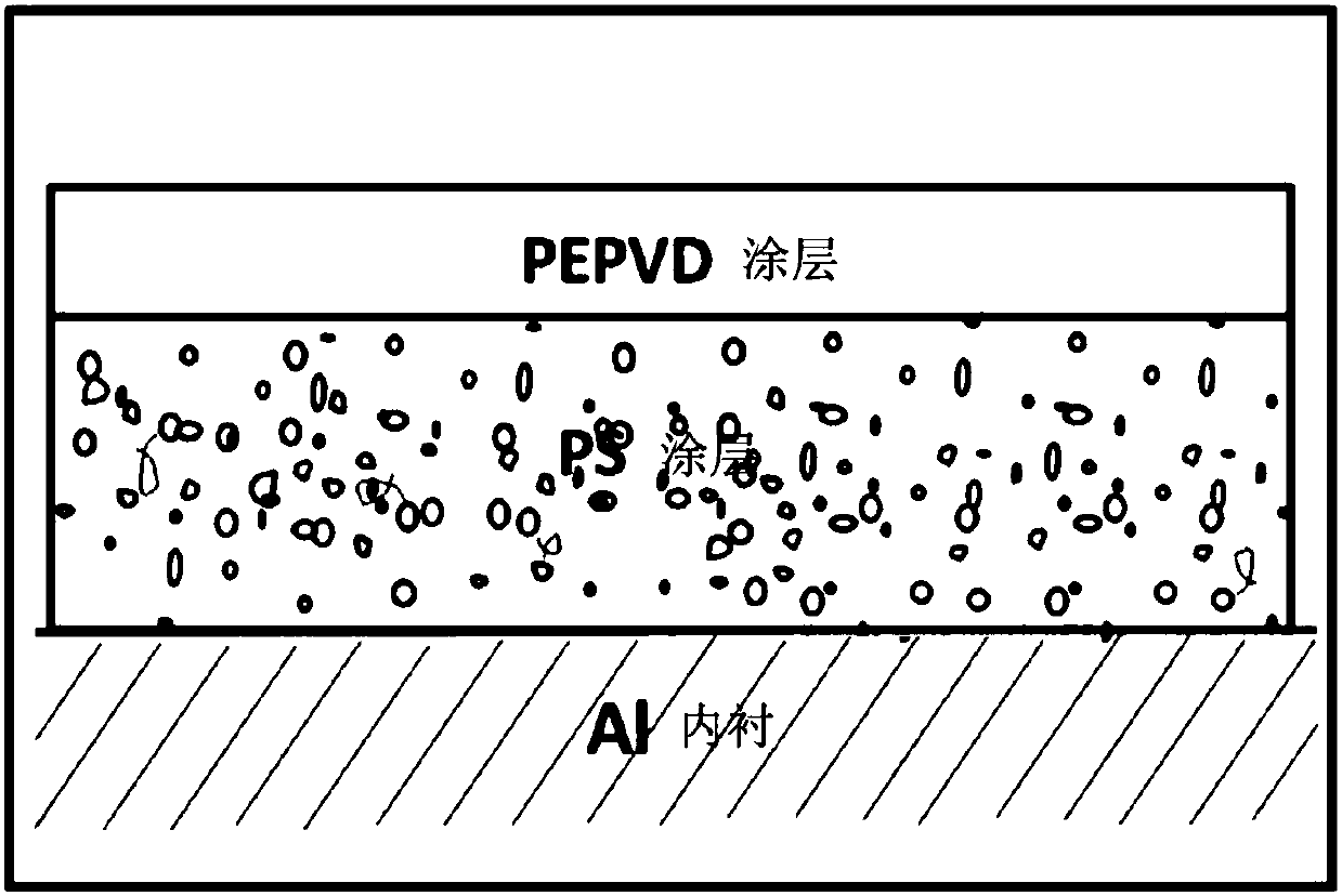
[0028] In a plasma etching chamber of the present invention, in this embodiment, the above-mentioned plasma etching chamber is an ICP chamber, and the inner wall surface is provided with a dense and smooth coating, and the coating is made of ceramic powder as the base material , and plasma spraying (PS) is used on the inner wall surface of the ICP cavity to generate a layer of composition Y 2 O 3 or YF 3coating. Then, polishing treatment is performed on the surface of the above-mentioned coating layer, so that the surface roughness (Ra) of the above-mentioned coating layer is less than 1 μm.

[0029] In this embodiment, using ceramic powder with a particle size of 10 μm or a smaller particle size as the substrate, the coating generated by PS can reduce the porosity and surface roughness, so that the porosity of ...


PUM


Abstract

The invention discloses a plasma etching reactor. The reactor comprises a cavity, a to-be-treated substrate is arranged in a space formed through the surrounding of the cavity, an upper side of the substrate comprises a reaction space, the reaction gas and radio frequency power are conveyed to the reaction space to form plasma to etch the substrate, an anti-plasma coating is formed on an inner wall surface of the cavity, thereby preventing plasma for etching a wafer in the cavity from corroding, and the roughness of a surface material layer of the anti-plasma coating is not more than 1 micron,and the porosity of the surface material layer of the anti-plasma coating is lower than 1%, and the thickness is greater than 10 microns; and the surface material layer of the anti-plasma coating iscomposed of compound including fluorine and yttrium. The reactor disclosed by the invention has the advantages of improving the structure stability of the internal surface of the plasma cavity or thecavity inner wall surface, improving the performance of the plasma etching process, satisfying a requirement of an advanced plasma etching process and reducing the production cost.

Description

technical field [0001] The present invention relates to the technical field of semiconductor equipment, in particular to a plasma etching reactor which can improve the performance of the plasma etching cavity of the semiconductor device by coating the inner wall of the cavity component of the semiconductor device with a coating. Background technique [0002] For inductive coupled plasma (ICP) and capacitive coupled plasma (CCP) etching chambers, the inner wall of the chamber is used to seal the plasma in the plasma reactor. Inside, during the plasma etching process, the large surface of the entire cavity is exposed to the plasma environment, and if the composition or properties of the surface of the inner wall of the cavity change, it will sensitively affect the plasma etching process stability. Usually, the inner wall of the cavity is made of aluminum alloy (Al alloy), and the surface of the inner wall of the cavity is covered with Y 2 O 3 Plasma spray coating or other p...

Claims


Application Information

Patent Timeline
Patent Type & Authority Applications(China)
IPC IPC(8): H01J37/32
CPCH01J37/32495H01J37/321
Inventor 贺小明陈星建刘身健倪图强
Owner ADVANCED MICRO FAB EQUIP INC CHINA
Why Eureka
Try Eureka