GaN-based light-emitting diode epitaxial wafer, preparation method of GaN-based light-emitting diode epitaxial wafer, and light-emitting diode

A technology of light-emitting diodes and epitaxial wafers, applied in the field of epitaxy, can solve the problems of reducing device performance, large compressive stress, low surface mobility dislocation density and cracks, and achieve the effect of suppressing the generation of dislocations and reducing the density

Active Publication Date: 2019-06-21
HC SEMITEK ZHEJIANG CO LTD
View PDF5 Cites 3 Cited by
  • Summary
  • Abstract
  • Description
  • Claims
  • Application Information

AI Technical Summary

Problems solved by technology

[0004] However, there is a large compressive stress between the AlN thin film buffer layer and GaN due to lattice mismatch and thermal mismatch, and the low surface mobility of Al atoms will generate a large number of dislocation densities and cracks inside the subsequent GaN. Defects will extend to the subsequent quantum well active area, greatly reducing the performance of the device

Method used


Image

  • GaN-based light-emitting diode epitaxial wafer, preparation method of GaN-based light-emitting diode epitaxial wafer, and light-emitting diode
  • GaN-based light-emitting diode epitaxial wafer, preparation method of GaN-based light-emitting diode epitaxial wafer, and light-emitting diode
  • GaN-based light-emitting diode epitaxial wafer, preparation method of GaN-based light-emitting diode epitaxial wafer, and light-emitting diode

Examples


Embodiment Construction

[0027] In order to make the object, technical solution and advantages of the present invention clearer, the implementation manner of the present invention will be further described in detail below in conjunction with the accompanying drawings.

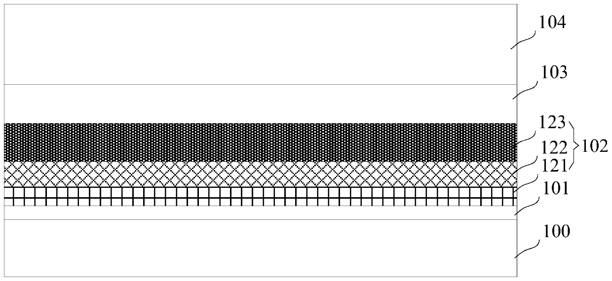
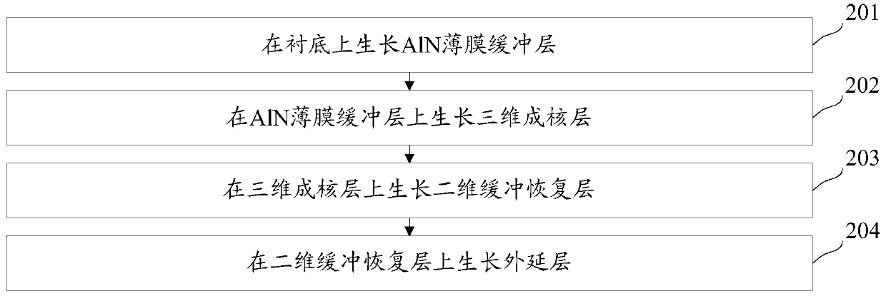
[0028] figure 1 It is a schematic structural diagram of a GaN-based light-emitting diode epitaxial wafer according to an embodiment of the present invention. see figure 1 , the GaN-based light-emitting diode epitaxial wafer includes a substrate 100 , and an AlN film buffer layer 101 , a three-dimensional nucleation layer 102 , a two-dimensional buffer recovery layer 103 and an epitaxial layer 104 stacked on the substrate 100 in sequence. Wherein, the three-dimensional nucleation layer 102 is a GaN layer; the three-dimensional nucleation layer 102 may include a first nucleation sublayer 121 , a second nucleation sublayer 122 and a third nucleation sublayer 123 sequentially stacked on the AlN film buffer layer 101 .

[0029] Wherein, t...


PUM

PropertyMeasurementUnit
thicknessaaaaaaaaaa
thicknessaaaaaaaaaa
thicknessaaaaaaaaaa

Abstract

The invention discloses a GaN-based light-emitting diode epitaxial wafer, a preparation method of the GaN-based light-emitting diode epitaxial wafer, and a light-emitting diode, and belongs to the technical field of epitaxy. The GaN-based light-emitting diode epitaxial wafer comprises a substrate, an AlN thin-film buffer layer, a three-dimensional nucleating layer, a two-dimensional buffer recovery layer and an epitaxial layer, wherein the AlN thin-film buffer layer, the three-dimensional nucleating layer, the two-dimensional buffer recovery layer and the epitaxial layer are sequentially stacked on the substrate; the three-dimensional nucleating layer is a GaN layer; the three-dimensional nucleating layer comprises a first nucleating sub-layer, a second nucleating sub-layer and a third nucleating sub-layer which are sequentially stacked on the AlN thin-film buffer layer; for the first nucleating sub-layer, the growth pressure of is 150-250 torr, the growth temperature is 1,000-1,100 DEG C, and the V/III ratio is 500-1,000; for the second nucleating sub-layer, the growth pressure is 500-700 torr, the growth temperature is 900-1,000 DEG C, and the V/III ratio is 100-200; and for thethird nucleating sub-layer, the growth pressure is 100-200 torr, the growth temperature is 1,100-1,150 DEG C, and the V/III ratio is 200-300. The interaction of dislocation is enhanced by growing thenucleating layer according to the three sub-layers, so that various dislocations caused by a pressure stress between the AlN thin-film buffer layer and GaN can be reduced, and the surface mobility ofAl atoms is improved.

Description

technical field [0001] The invention relates to the field of epitaxy technology, in particular to a GaN-based light-emitting diode epitaxial wafer, a preparation method thereof, and a light-emitting diode. Background technique [0002] Currently, Gallium Nitride (GaN)-based Light Emitting Diodes (Light Emitting Diodes, LEDs) are receiving more and more attention and research. Epitaxial wafer is the core part of GaN-based LED. The structure of epitaxial wafer includes: substrate, buffer layer, three-dimensional nucleation layer, two-dimensional buffer recovery layer and epitaxial layer. [0003] In the process of blue light and white light LED, most of the substrates are sapphire substrates, and there are always problems of lattice mismatch and thermal mismatch between sapphire substrates and GaN materials. The study found that since there is only a small lattice mismatch between the aluminum nitride (AlN) material and the sapphire substrate, placing the AlN film buffer laye...

Claims


Application Information

Patent Timeline
Patent Type & Authority Applications(China)
IPC IPC(8): H01L21/02H01L33/00C23C14/35C23C14/06C23C16/30C23C16/44
Inventor 陶章峰程金连曹阳乔楠胡加辉李鹏
Owner HC SEMITEK ZHEJIANG CO LTD
Why Eureka
Try Eureka