A method for regulating vacancy defects in materials

A technology of vacancy defects and functional materials, applied in the field of microelectronic materials, can solve problems such as performance failure and formation of voids, and achieve the effect of improving speed, improving speed of erasing and writing, and mature technology

Active Publication Date: 2020-08-18
HUAZHONG UNIV OF SCI & TECH
View PDF5 Cites 0 Cited by
  • Summary
  • Abstract
  • Description
  • Claims
  • Application Information

AI Technical Summary

Problems solved by technology

On the other hand, the existence of vacancies will form voids in the process of repeated erasing and writing of phase change memory materials, leading to their performance failure, which may be an important factor limiting the cycle erasing ability of phase change materials (Njoroge W K, H W, Wuttig M. Density changes upon crystallization of Ge 2 Sb 2.04 Te 4.74 films[J].Journal of Vacuum Science&Technology A:Vacuum, Surfaces, and Films,2002,20(1):230-233.)

Method used


Image

  • A method for regulating vacancy defects in materials
  • A method for regulating vacancy defects in materials
  • A method for regulating vacancy defects in materials

Examples


Embodiment 1

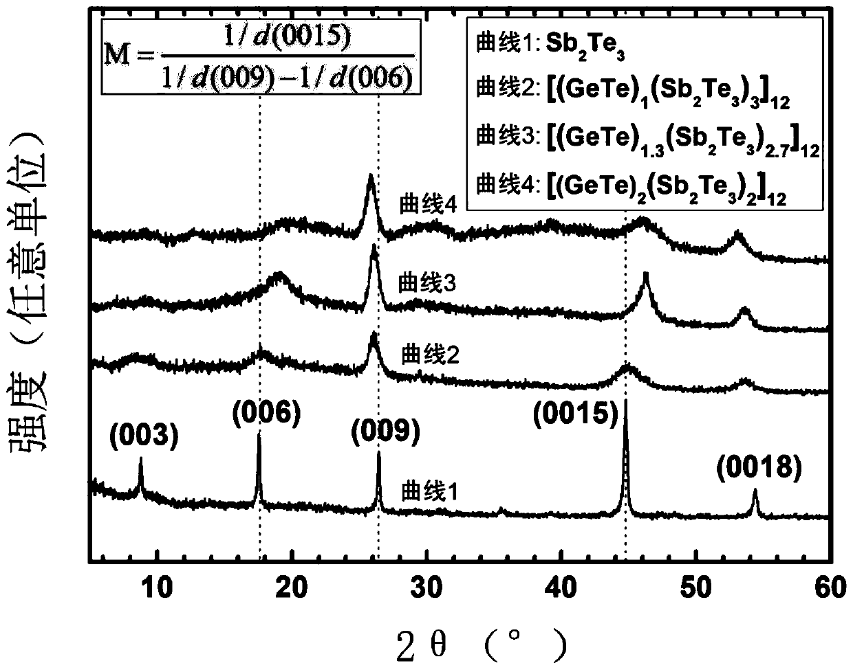
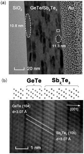
[0049] The structure of the multilayer phase change stress film prepared in the present embodiment is [A m B n ] l , where m and n represent the thicknesses of A and B respectively, the default unit is nm (nanometer), and l is the number of cycles of alternate growth of the multilayer film. 1 / 102 Te 3 , m / n are 4 / 0, 2 / 2, 1.3 / 2.7, 1 / 3 respectively, and l is 12. GeTe is a microscopic non-layered material with no van der Waals gap. Sb 2 Te 3 It is a microscopic layered material containing van der Waals gap, and its crystallization temperature is lower than that of GeTe, and it will crystallize before GeTe in the phase transition process. Therefore, the crystallization characteristics of the multilayer film (such as SET speed, etc.) are mainly determined by the slower crystallization speed of GeTe. Sb 2 Te 3 Although the crystallization of the multilayer film does not play a decisive role in the crystallization process of the multilayer film, it can exert stress on GeTe t...

Embodiment 2

[0087] In this embodiment, the multi-layer stress thin film structure is prepared as a phase change unit, and the SET speed test is carried out. Multilayer film [A m B n ] l A is still GeTe, B is still Sb 2 Te 3 , GeTe and Sb 2 Te 3 The thickness ratio is still: 4 / 0, 2 / 2, 1.3 / 2.7, 1 / 3, and the number of cycles is still fixed at 12. The preparation process of the multilayer film structure phase change unit is as follows:

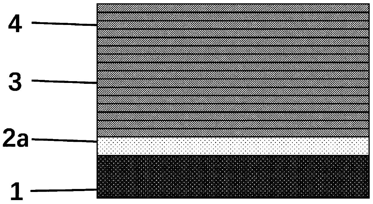
[0088] (1) if Figure 5 As shown in (a), on the substrate composed of layer 1 and layer 2a, the lower electrode 5a layer is first deposited by magnetron sputtering, and the 5a layer is made of inert electrode materials such as Pt, TiW, and Ta.

[0089] (2) Deposit insulating layer 2b on layer 5a by physical vapor deposition (PECVD), layer 2b is SiO 2 , SiC, Al 2 o 3 and other insulating materials.

[0090](3) A photoresist mask with circular holes with a diameter of 250 nm was formed on the insulating layer 2 b by using an electron beam exposure s...


PUM

PropertyMeasurementUnit
thicknessaaaaaaaaaa
sizeaaaaaaaaaa

Abstract

The invention discloses a method for regulating a vacancy defect of a material. The method, by inserting a stress applying material into a phase change functional material, regulates the vacancy defect concentration in the phase change functional material, and thus obtains a composite structure formed by the embedded growth of the phase change functional material and the stress applying material.The phase change property of the composite structure is mainly determined by the phase change functional material therein. By the regulation of the stress applying material, the phase change propertyof the composite structure varies on the basis of the phase change property of the phase change functional material crystal obtained by the pure phase change functional material, and the stress application material is specifically a material capable of forming a crystalline state. In particular by inserting the stress applying material having a slightly larger lattice constant into the phase change functional material having a slightly smaller lattice constant, the method can reduce the vacancy defect concentration of the phase change memory material, thereby lowering the threshold of the crystallization process and increasing the crystallization speed.

Description

technical field [0001] The invention belongs to the field of microelectronic materials, and more specifically relates to a method for regulating vacancy defects in materials. The method can actively modulate material defects, and in particular can regulate vacancy defects in phase-change storage materials. Background technique [0002] Phase-change memory materials have attracted much attention because they can quickly realize reversible transformation between low-resistance state and high-resistance state by applying electricity or light pulses. The process of changing from high resistance to low resistance is called SET process. The process is called the RESET process. Storage technology based on phase-change materials is considered to be one of the strong competitors of next-generation storage technology. Phase-change memory devices have the advantages of fast erasing and writing speeds, large differences between two states, and compatibility with existing complementary ...

Claims


Application Information

Patent Timeline
Patent Type & Authority Patents(China)
IPC IPC(8): H01L45/00
Inventor 程晓敏冯金龙缪向水
Owner HUAZHONG UNIV OF SCI & TECH
Why Eureka
Try Eureka