Supercharge Your Innovation With Domain-Expert AI Agents!

Er or Er/O doped silicon based room-temperature communication waveband luminescent material, preparation method thereof and silicon-based laser

A luminescent material and laser technology, applied in the field of silicon-based semiconductor process processing and silicon-based luminescent material preparation, can solve the problems of non-radiative transition quenching and low luminous efficiency, and achieve the effect of important industrial application value

Pending Publication Date: 2019-06-25
SHANGHAI JIAO TONG UNIV
View PDF3 Cites 1 Cited by
  • Summary
  • Abstract
  • Description
  • Claims
  • Application Information

AI Technical Summary

Problems solved by technology

However, silicon materials doped with erbium or erbium oxygen still have defects such as non-radiative transition quenching at room temperature, and the luminous efficiency is extremely low, which has become the only technical bottleneck for its industrial application.

Method used


Image

  • Er or Er/O doped silicon based room-temperature communication waveband luminescent material, preparation method thereof and silicon-based laser
  • Er or Er/O doped silicon based room-temperature communication waveband luminescent material, preparation method thereof and silicon-based laser
  • Er or Er/O doped silicon based room-temperature communication waveband luminescent material, preparation method thereof and silicon-based laser

Examples


Embodiment Construction

[0023] In the following description, numerous specific details are set forth in order to provide a thorough understanding of the invention. The present invention may be practiced without some or all of these specific details. In other instances, well known process operations have not been described in detail in order not to unnecessarily obscure the present invention. While the invention will be described in conjunction with specific embodiments, it will be understood that they are not intended to limit the invention to those embodiments.

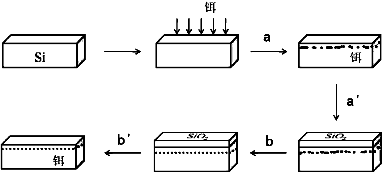
[0024] figure 1 It is a flow chart of a preparation method of an erbium- or erbium-oxygen-doped silicon-based room-temperature communication-band luminescent material (hereinafter referred to as "erbium- or erbium-oxygen-doped silicon-based luminescent material") according to an embodiment of the present invention. Such as figure 1 As shown, the preparation method of the erbium (or erbium oxide) silicon-based luminescent material of the ...


PUM

PropertyMeasurementUnit
thicknessaaaaaaaaaa
diameteraaaaaaaaaa
quantum efficiencyaaaaaaaaaa

Abstract

luminescent material an Er or Er / O doped silicon based room-temperature communication waveband luminescent material and a preparation method thereof. The preparation method comprises the following steps that a) erbium ion implantation doping or erbium and oxygen ion implantation co-doping is carried out on a monocrystalline silicon chip to obtain an Er-doped or Er / O-doped silicon chip; and b) cryogenic annealing, including a heating process and a rapid cooling process, is carried out on the Er-doped or Er / O-doped silicon chip. According to the preparation method, the silicon-based semiconductor material can realize high-efficiency room temperature photoluminescence in the waveband of 1.53micron by means of the cryogenic annealing technology, and a feasible technical means is provided for successful preparation for silicon luminescence and silicon laser light sources. The whole technical process is compatible with CMOS technology, and the industrial application value is high. The invention further provides an Er-doped or Er / O-doped silicon-based room temperature communication waveband laser based on the cryogenic annealing technology.

Description

technical field [0001] The invention belongs to the technical field of semiconductor silicon photoelectricity, and relates to a new method for silicon-based semiconductor process treatment, in particular to a method for preparing silicon-based light-emitting materials doped with erbium or erbium-oxygen. Background technique [0002] The realization of silicon-based photonic integration technology and silicon-based optoelectronic integration technology can break through the bottleneck of current microelectronics technology development. The use of silicon-based materials to manufacture high-quality, high-efficiency room temperature communication band light-emitting devices is of great significance to optoelectronics and even the entire field of information technology. Due to the limitation of the indirect bandgap energy band structure, intrinsic silicon materials show very low luminescence characteristics, and silicon-based light sources cannot be realized in principle. At pr...

Claims


Application Information

Patent Timeline
Patent Type & Authority Applications(China)
IPC IPC(8): H01S5/30H05B6/02
Inventor 但亚平文惠敏何佳晶
Owner SHANGHAI JIAO TONG UNIV
Features
  • R&D
  • Intellectual Property
  • Life Sciences
  • Materials
  • Tech Scout
  • Unparalleled Data Quality
  • Higher Quality Content
  • 60% Fewer Hallucinations
Learn More