A kind of fabrication method of columnar coaxial ring nanostructure

A nanostructure and manufacturing method technology, applied in the field of micro-nanostructure preparation, can solve the problems of high cost, reduced freedom of nano-imprinting, low efficiency, etc., and achieve the effects of high processing freedom and low cost

Active Publication Date: 2021-06-15
SOUTH CHINA NORMAL UNIVERSITY
View PDF9 Cites 0 Cited by
  • Summary
  • Abstract
  • Description
  • Claims
  • Application Information

AI Technical Summary

Problems solved by technology

Usually, the preparation of such nanoscale coaxial columnar structures mainly adopts processes such as focused ion beam etching (FIB), electron beam exposure (EBL), and nanoimprinting. The first two methods are extremely expensive and use point-by-point The scanning processing method is extremely inefficient when the sample area is large; while nanoimprinting can prepare coaxial nanostructures in a large area, the preparation of the template also needs to be realized by expensive and inefficient processes such as FIB and EBL, and the template Once prepared, it cannot be changed, which greatly reduces the freedom of subsequent nanoimprinting

Method used


Image

  • A kind of fabrication method of columnar coaxial ring nanostructure
  • A kind of fabrication method of columnar coaxial ring nanostructure
  • A kind of fabrication method of columnar coaxial ring nanostructure

Examples


Embodiment 1

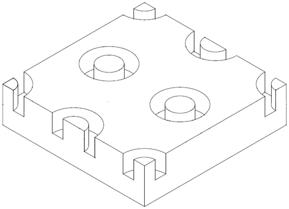
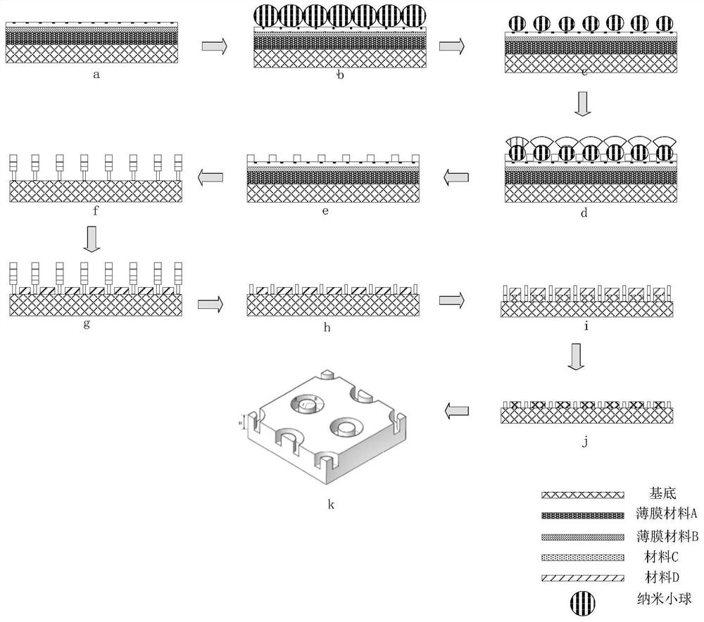
[0044] Figure 1-Figure 2 The manufacturing method of the shown columnar coaxial ring nanostructure, it may further comprise the steps:

[0045] (1) Film material A and film material B are coated successively on the silicon substrate, wherein, film material A is photoresist SU8 resistant to organic solvent corrosion, and film material B is positive resist Ar-P- 3740; and a layer of material C is plated on the upper surface of material B by physical deposition, and material C is titanium with a thickness of 30nm, such as figure 2 a.

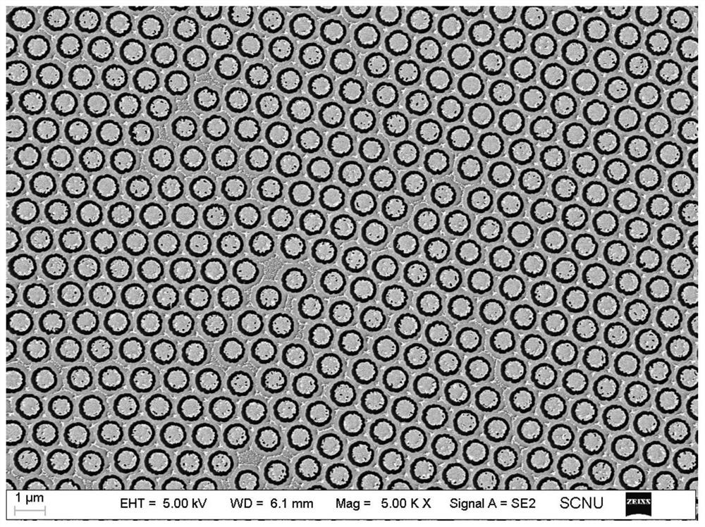
[0046] (2) the surface of the substrate after step (1) arranges a layer of polystyrene (PS) balls with a diameter of 1um by self-assembly method, such as figure 2 b, The size of the diameter of the spheres here will determine the period size of the final columnar coaxial nanostructure, or when the self-assembly process is controlled so that the spheres are randomly distributed, a randomly arranged columnar coaxial nanostructure can finally be ...

Embodiment 2

[0063] The difference between the manufacturing method of the columnar coaxial ring nanostructure in this embodiment and the embodiment 1 is that the substrate is a silicon dioxide substrate. Inductively Coupled Plasma Etching (ICP) etched silicon dioxide substrates using C 4 f 8 Mixed gas with He as the reaction gas. The specific etching process parameters are shown in Table 3:

[0064] Table 3 Process parameters of inductively coupled plasma etching (ICP) etching substrate silicon dioxide

[0065]

[0066] In this embodiment, the etching time of the base silicon dioxide is 190s.


PUM

PropertyMeasurementUnit
depthaaaaaaaaaa
thicknessaaaaaaaaaa
depthaaaaaaaaaa

Abstract

The invention provides a method for manufacturing a columnar coaxial ring nanostructure, comprising the step of forming a pattern etching layer on the substrate surface; processing the pattern etching layer to form a columnar coaxial ring nanostructure on the substrate surface ; Using the columnar coaxial ring nanostructure on the surface of the substrate as a mask, etching the substrate, transferring the structure to the substrate, and removing the surface structure of the substrate. The method is fast and efficient, and can be prepared in a large area; the cost is low, and the processing freedom is high.

Description

technical field [0001] The invention belongs to the field of preparation of micro-nano structures, and in particular relates to a preparation method of a columnar coaxial ring nano-structure. Background technique [0002] Nanotechnology is currently a major research hotspot. Various nanostructures exhibit many novel physical properties, and are considered to have great application potential in many fields such as optics, materials, biology, energy, and medicine. Columnar coaxial nanostructures are a special kind of nanostructures, especially after metallization, can be used to form special nano-optical resonant cavities, which can be used in refractive index sensing, surface Raman enhancement, nano-laser and other occasions. The scale of such columnar coaxial nanostructures is often on the order of tens of nanometers to several microns. When the outer diameter is within 1 micron, its preparation has high requirements on the processing technology. Usually, the preparation o...

Claims


Application Information

Patent Timeline
Patent Type & Authority Patents(China)
IPC IPC(8): B81C1/00
Inventor 黄广飞张渊胡治朋朱圣科刘柳
Owner SOUTH CHINA NORMAL UNIVERSITY
Why Eureka
Try Eureka