Diamond-like thin film solar cell and manufacturing method thereof

A diamond thin film and solar cell technology, applied in the field of solar cells, can solve problems such as current loss and low conversion efficiency

Inactive Publication Date: 2021-08-17
XIAMEN UNIV
View PDF4 Cites 0 Cited by
  • Summary
  • Abstract
  • Description
  • Claims
  • Application Information

AI Technical Summary

Problems solved by technology

At present, the conversion efficiency of diamond-like solar cells is low, and it is necessary to further improve the solar spectrum absorption efficiency of solar cells and avoid the current loss caused by multiple tunnel junctions.

Method used


Image

  • Diamond-like thin film solar cell and manufacturing method thereof
  • Diamond-like thin film solar cell and manufacturing method thereof
  • Diamond-like thin film solar cell and manufacturing method thereof

Examples


Embodiment 1

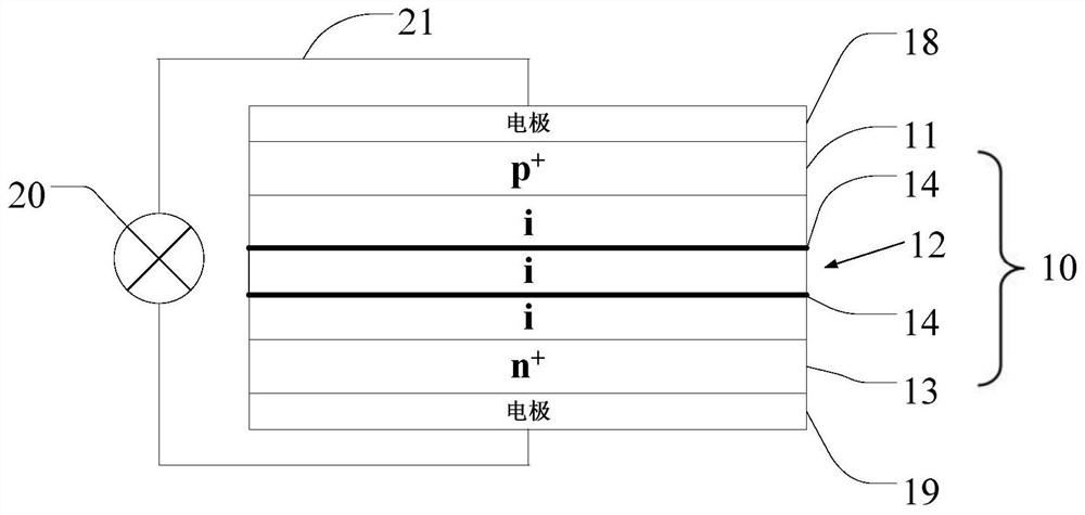
[0030] Now refer figure 1 , figure 1 It is a schematic diagram of a thin film solar cell, and according to an embodiment of the present invention, it has a Pin junction 10, and the Pin junction 10 includes an intrinsic layer 12 having a P + type layer 11, N + type layer 13, and a plurality of continuous laminated. The battery also includes an electrode 19 connected to an electrode 18 on one side of the P + -type layer 11 and an electrode 19 of the N + -type layer 13; wherein each of the P + -type layers 11 and N + layer 13 have different SP3. / SP2 ratio.

[0031] figure 1 In the schematic diagram of the solar cell, there is a continuous lamination of the intrinsic layer corresponding to the solar spectrum of the three bands of ultraviolet, visible light, and infrared, thereby achieving full spectral absorption, achieving higher solar cell photoelectric conversion efficiency. .

[0032] Each of the intrinsic layer 12 includes a plurality of quantum wells. The tunneling layer 12 i...

Embodiment 2

[0040] Specific structure of the diamond solar cell structure Reference Examples Such diamond solar cells have a PIN junction, and the PIN junction includes a P + type layer, a n + layer, and a plurality of continuous laminated intrinsic layers; and an electrode connected to one side of the P +-type layer and the N + type layer. The electrodes on one side are in which each of the intrinsic layers have different SP3 / SP2 ratios and corresponding disable band widths. The intrinsic layer is a diamond material, and the diamond material is a mixture of crystalline carbon and amorphous carbon.

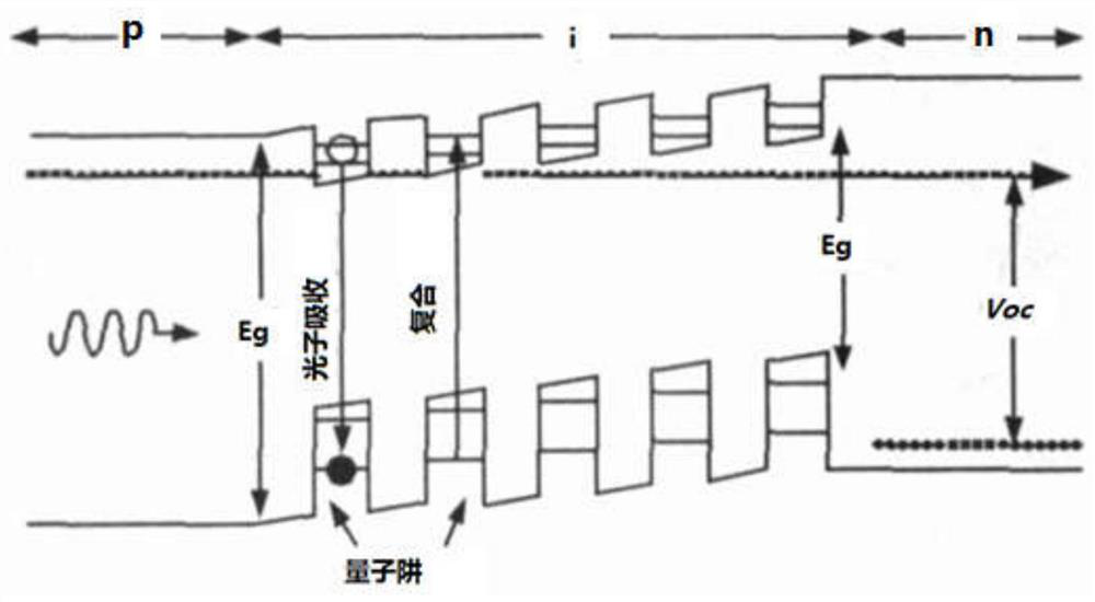
[0041] Each of the intrinsic layers includes one or more quantum wells. in, figure 2It is a quantum well energy level having a single intrinsic layer. The quantum well has a thickness of 3 to 10 nm, a superposition of 15 to 50 carbon atomic layers to achieve a higher solar cell photoelectric conversion efficiency. As shown in the figure, the solar photon enters the intrinsic layer from the P + ...

Embodiment approach

[0050] According to an embodiment of the present invention, there is provided a method for manufacturing a diamond thin film solar cell, including the following steps:

[0051] (a) introducts the hydrocarbon (such as: methane) into the deposition chamber to form a first electrode layer, thereby generating a Pin junction having a plurality of continuous laminated intrinsic layers, the PIN junction having p + Type layer, N + type layer and intrinsic layer;

[0052] (b) Changes at least the SP3 / SP2 ratio of each P + -type layer and N +-type layer, which can be doped to enhance the electronic mobility in each PIN;

[0053] (c) The second electrode layer is manufactured according to step a and b;

[0054] Among them, a plurality of consecutive laminated intrinsic layers are close to each other in step (a) to produce a solar cell having an optimized spectral response and an optimized thermal response to the direction of the direction of the light source.

[0055] figure 2 It is a gra...


PUM

PropertyMeasurementUnit
thicknessaaaaaaaaaa
diameteraaaaaaaaaa

Abstract

The present invention provides a diamond-like thin film solar cell, which includes: a pin junction, the pin junction includes a p+ type layer, an n+ type layer and a plurality of successively stacked intrinsic layers; and a junction connected to the p+ type layer An electrode on one side and an electrode connected to one side of the n+ type layer; wherein, in the plurality of successively stacked intrinsic layers, each of the intrinsic layers has a different sp3 / sp2 ratio and a corresponding forbidden band width; the intrinsic layer is a diamond-like material. The pin junction of the diamond-like thin film solar cell provided by the present invention has a plurality of successively stacked intrinsic layers to realize full solar spectrum absorption and avoid current loss caused by multiple tunnel junctions.

Description

Technical field [0001] The present invention relates to the field of solar cells, and in particular, the present invention relates to a full spectral diamond quantum well film solar cell and a method of manufacturing the same. Background technique [0002] In recent years, chemical vapor deposition (CVD) diamond (class diamond) films have been greatly developed. The uniqueness of the diamond membrane is similar to the nature of single crystal block diamond, including: high hardness, low friction coefficient, chemical inert, transparency, high resistivity and smoothness; this makes it suitable for many applications. Because the banned bandwidth of the diamond itself is continuously adjustable within 0 to 5.4 eV, there is a unique application in the solar cell. At present, the conversion efficiency of the Class diamond solar cell is low, and it is necessary to further improve solar spectroscopy efficiency of solar cells, and avoid the current loss caused by multiple tunnels. Inven...

Claims


Application Information

Patent Timeline
Patent Type & Authority Patents(China)
IPC IPC(8): H01L31/077H01L31/028H01L31/0376H01L31/0392H01L31/18
CPCY02E10/547Y02P70/50
Inventor 何嵩张彬彬
Owner XIAMEN UNIV
Why Eureka
Try Eureka