Gallium nitride-based LED epitaxial wafer and manufacturing method thereof

A light-emitting diode, gallium nitride-based technology, applied in the direction of electrical components, circuits, semiconductor devices, etc., can solve the problems of aggravated electron leakage, efficiency decline, LED luminous efficiency reduction, etc., to improve luminous efficiency, prevent electron leakage, suppress The effect of light effect reduction

Inactive Publication Date: 2019-06-28
HC SEMITEK SUZHOU
View PDF3 Cites 12 Cited by
  • Summary
  • Abstract
  • Description
  • Claims
  • Application Information

AI Technical Summary

Problems solved by technology

And as the current increases, the leakage of electrons will be aggravated, which will further reduce the luminous efficiency of the LED. This phenomenon is called Efficiency droop (efficiency decline)

Method used


Image

  • Gallium nitride-based LED epitaxial wafer and manufacturing method thereof
  • Gallium nitride-based LED epitaxial wafer and manufacturing method thereof

Examples


Embodiment Construction

[0028] In order to make the object, technical solution and advantages of the present invention clearer, the implementation manner of the present invention will be further described in detail below in conjunction with the accompanying drawings.

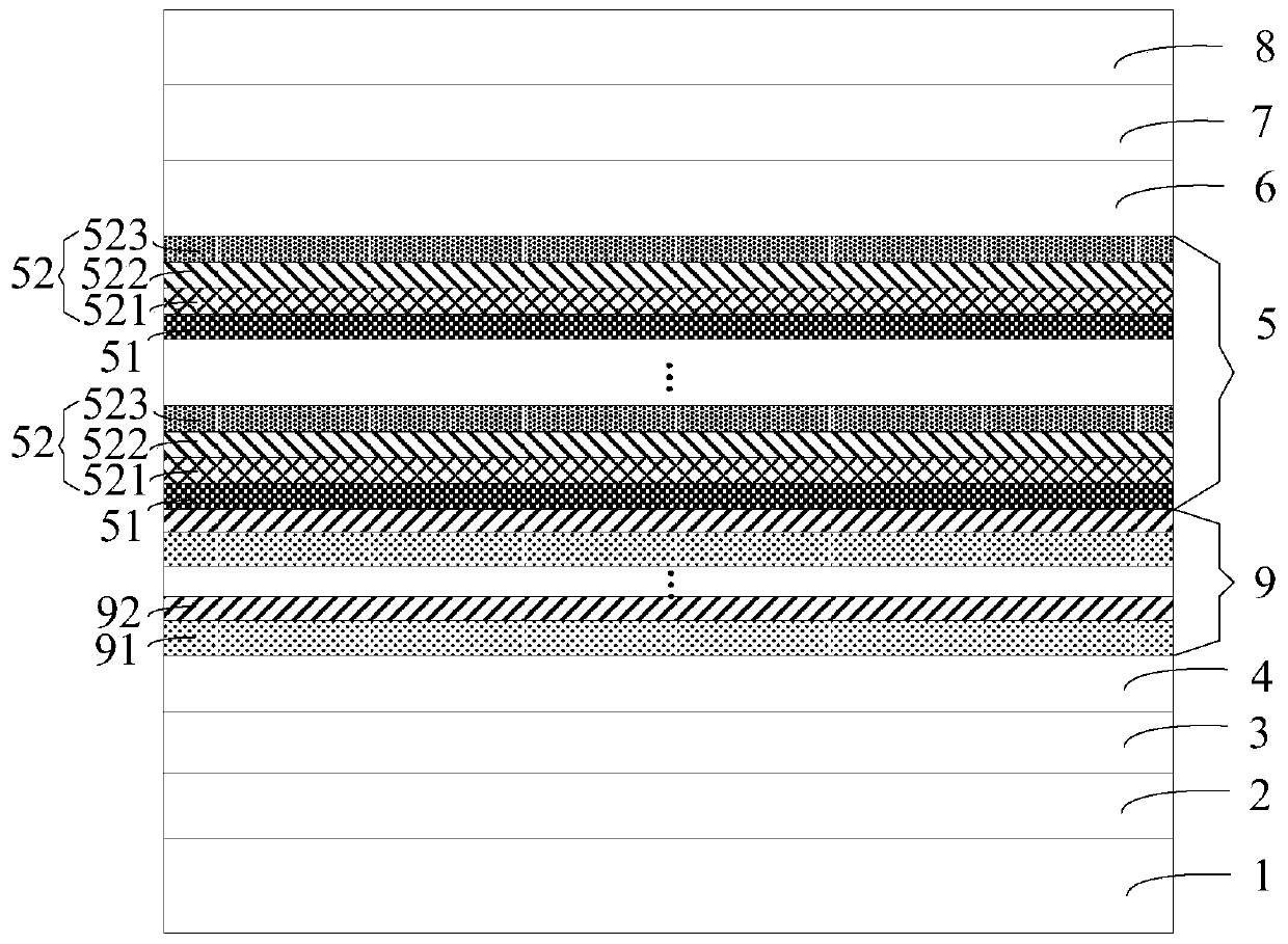
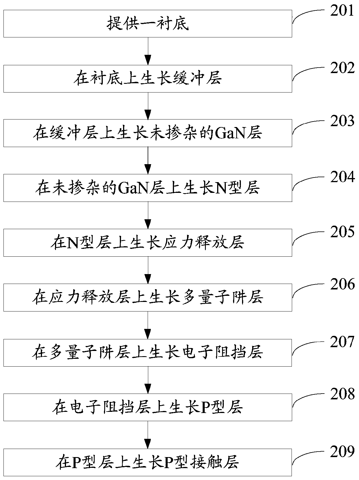
[0029] figure 1 It is a schematic structural diagram of a gallium nitride-based light-emitting diode epitaxial wafer provided by an embodiment of the present invention, as shown in figure 1 As shown, the GaN-based light-emitting diode epitaxial wafer includes a substrate 1, a buffer layer 2 grown on the substrate 1 in sequence, an undoped GaN layer 3, an N-type layer 4, a multi-quantum well layer 5, and an electron barrier Layer 6, P-type layer 7 and P-type contact layer 8.

[0030] The multi-quantum well layer 5 includes alternately grown InGaN quantum well layers 51 and composite quantum barrier layers 52, and the composite quantum barrier layer 52 includes sequentially stacked first quantum barrier layers 521, second quantum barrie...


PUM


Abstract

The invention discloses a gallium nitride-based LED epitaxial wafer and a manufacturing method thereof, and belongs to the technical field of semiconductors. The gallium nitride-based LED epitaxial wafer includes a substrate, and a group including a buffer layer, an undoped GaN layer, an N-type layer, a multi-quantum well layer, an electron barrier layer, a P-type layer, and a P-type contact layerwhich are successively grown on the substrate, wherein the multi-quantum quantum well layer comprises alternately grown InGaN quantum well layers and composite quantum barrier layers; each compositequantum barrier layer comprises a first quantum barrier layer, a second quantum barrier layer and a third quantum barrier layer which are successively stacked; the first quantum barrier layer and thethird quantum barrier layer are both AlInGaN layers; the second quantum barrier layer is an AlGaN layer; and the Al components in the second quantum barrier layer gradually increases and then gradually decreases along the stacking direction of the epitaxial wafer. The LED epitaxial wafer provided by the invention can suppress a decrease in the luminous efficiency of the LED under large current injection and improve the luminous efficiency of the LED.

Description

technical field [0001] The invention relates to the technical field of semiconductors, in particular to a gallium nitride-based light-emitting diode epitaxial wafer and a manufacturing method thereof. Background technique [0002] LED (Light Emitting Diode, Light Emitting Diode) is a semiconductor electronic component that can emit light. As an efficient, environmentally friendly and green new solid-state lighting source, it is being rapidly and widely used, such as traffic lights, car interior and exterior lights, urban landscape lighting, mobile phone backlights, etc. [0003] Epitaxial wafers are the main components of LEDs. Existing GaN-based LED epitaxial wafers include substrates, buffer layers, undoped GaN layers, N-type layers, multiple quantum well layers, electron barrier layer and P-type layer. Wherein, the multi-quantum well layer includes alternately grown InGaN quantum well layers and GaN quantum barrier layers. [0004] In the process of realizing the prese...

Claims


Application Information

Patent Timeline
Patent Type & Authority Applications(China)
IPC IPC(8): H01L33/00H01L33/06H01L33/32
Inventor 丁杰秦双娇胡任浩周飚胡加辉
Owner HC SEMITEK SUZHOU
Why Eureka
Try Eureka