P-type tunneling oxide passivated contact solar cell and preparation method thereof

A technology of solar cells and oxides, applied in circuits, photovoltaic power generation, electrical components, etc., can solve the problems of poor passivation effect on the back of solar cells, and achieve excellent interface passivation effect, high conversion efficiency, and high temperature stability Effect

Pending Publication Date: 2019-07-05
TONGWEI SOLAR ENERGY CHENGDU CO LID
View PDF0 Cites 11 Cited by
  • Summary
  • Abstract
  • Description
  • Claims
  • Application Information

AI Technical Summary

Problems solved by technology

[0004] The purpose of the present invention is to solve the problem of poor passivation effect on the back of solar cells in the prior art, to provide a P-type tunneling oxide passivated contact solar cell with better passivation effect and higher conversion efficiency and its preparation method

Method used


Image

  • P-type tunneling oxide passivated contact solar cell and preparation method thereof
  • P-type tunneling oxide passivated contact solar cell and preparation method thereof

Examples


preparation example Construction

[0040] A method for preparing a P-type tunnel oxide passivation contact solar cell, the preparation of the P-type tunnel oxide passivation contact solar cell comprises the following steps:

[0041] S1. First remove the damaged layer of the silicon wafer and then use the alkali texturing process to form a pyramid textured surface with a height of 0.5 μm-5 μm;

[0042] S2, using phosphorus oxychloride (POCl 3 ) high-temperature diffusion, the reaction temperature is 750-850°C, and the reaction time is 30-60min, forming a P-doped N+ emitter junction on the surface of the silicon wafer, that is, an N-type heavily doped silicon layer, and forming a phosphosilicate glass (PSG) layer at the same time.

[0043] S3, cleaning the silicon wafer surface;

[0044] S31, using HF solution to remove the phosphosilicate glass (PSG) layer on the surface of the silicon wafer;

[0045] S32, using the RCA wet chemical method to clean the surface of the silicon wafer;

[0046] S4, using low-pres...

Embodiment 1

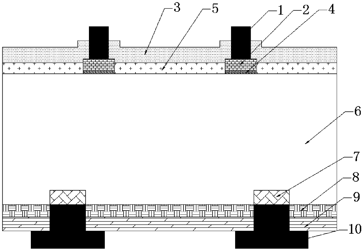
[0054] A P-type tunneling oxide passivation contact solar cell, including a front electrode, an anti-reflection layer 1, an N-type heavily doped silicon layer, a P-type silicon substrate, an Al 2 o 3 Passivation layer, anti-reflection layer two, back electrode, said anti-reflection layer one, N-type heavily doped silicon layer, P-type silicon substrate, Al 2 o 3 The passivation layer, anti-reflection layer 2, and the back electrode are stacked in sequence, and the N-type heavily doped silicon layer is also stacked with an N-type heavily doped polysilicon layer and SiO 2 layer, SiO 2 The layer is arranged in contact with the P-type silicon substrate, and the front electrode penetrates the anti-reflection layer to be in contact with the N-type heavily doped polysilicon layer.

[0055] Among them, the P-type silicon substrate is close to the Al 2 o 3 The back of the passivation layer is embedded with a P-type heavily doped silicon layer, and the back electrode passes through...

Embodiment 2

[0071] On the basis of Example 1, the preparation method for preparing a P-type tunnel oxide passivation contact solar cell in this example includes the following steps:

[0072] S1. First remove the damaged layer of the silicon wafer and then use the alkali texturing process to form a 3 μm high pyramid textured surface;

[0073] S2, using phosphorus oxychloride (POCl 3 ) High-temperature diffusion, the reaction temperature is 800°C, and the reaction time is 45 minutes, forming a P-doped N+ emitter junction on the surface of the silicon wafer, that is, an N-type heavily doped silicon layer, and forming a phosphosilicate glass (PSG) layer at the same time;

[0074] S3, cleaning the silicon wafer surface;

[0075] S31, using HF solution to remove the phosphosilicate glass (PSG) layer on the surface of the silicon wafer;

[0076] S32, using the RCA wet chemical method to clean the surface of the silicon wafer;

[0077] S4, using low-pressure chemical vapor deposition (LPCVD) o...


PUM


Abstract

The invention discloses a P-type tunneling oxide passivated contact solar cell and belongs to the technical field of crystalline silicon solar cells, aiming to solve the problem that the passivation effect of the back surface of the solar cell in the prior art is poor; the solar cell in the invention is characterized in that a silicon dioxide layer is formed on the front surface of a silicon wafer, and then an N-type heavily-doped polycrystalline silicon layer is formed on the silicon dioxide layer, so that the composite loss of a metal contact area is reduced; in addition, the tunneling oxideis combined with a heavily-doped silicon thin film to form a passivated contact structure, so that the original way of whole-face doping the back surface area is replaced, further, a high short-circuit current is kept, the open-circuit voltage is increased, the filling factor is improved, and the conversion efficiency of the battery is improved.

Description

technical field [0001] The invention belongs to the technical field of crystalline silicon solar cells, and in particular relates to a P-type tunneling oxide passivation contact solar cell and a preparation method thereof. Background technique [0002] At present, solar cells mainly use crystalline silicon as the base material. Due to periodic damage on the surface of the silicon wafer, a large number of dangling bonds will be generated, so that there are a large number of defect levels in the band gap on the crystal surface; in addition, Dislocations, chemical residues, and surface metal deposition will all lead to defect energy levels, making the surface of the silicon wafer a recombination center, resulting in a large surface recombination rate, which in turn limits the conversion efficiency. Back passivated solar cells coated with SiN on the front x , back-coated Al 2 o 3 、SiN x Layering, reducing the rate of surface recombination has a general effect. In addition, ...

Claims


Application Information

Patent Timeline
Patent Type & Authority Applications(China)
IPC IPC(8): H01L31/0216H01L31/18
CPCH01L31/02167H01L31/02168H01L31/1876Y02E10/50Y02P70/50
Inventor 吴俊旻洪布双张鹏尹丙伟王岚张元秋
Owner TONGWEI SOLAR ENERGY CHENGDU CO LID
Why Eureka
Try Eureka