Silicon chip oxidation method

A silicon wafer, ozone oxidation technology, applied in photovoltaic power generation, sustainable manufacturing/processing, electrical components, etc., can solve the problems of low ozone oxidation level and uniformity, poor ozone stability, and reduced oxidation performance, etc., to improve the interface Passivation effect, improved efficiency, improved oxidation uniformity effect

Inactive Publication Date: 2016-09-07
ZHEJIANG JINKO SOLAR CO LTD +1
View PDF4 Cites 4 Cited by
  • Summary
  • Abstract
  • Description
  • Claims
  • Application Information

AI Technical Summary

Problems solved by technology

Specifically, the silicon wafer is placed on the supporting column of the silicon wafer stage of the etching device, and then the lid of the etching chamber is closed, and ozone enters the sealed etching chamber, contacts the surface of the silicon wafer, and oxidizes the surface of the silicon wafer into a dense oxide film. However, this technology has the following disadvantages: due to the poor stability of ozone at normal temperature and pressure, it can be decomposed into oxygen by itself, resulting in a decrease in oxidation performance, and the ozone gas is in direct contact with the silicon wafer during the reaction, and it is sprayed by airflow during gaseous oxidation. Inhomogeneous, so the oxidation level and uniformity of the ozone is not high

Method used


Image

  • Silicon chip oxidation method

Examples


Embodiment Construction
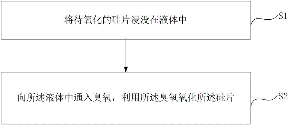
[0022] The core idea of ​​the present invention is to provide a silicon wafer oxidation method, which can improve the ozone oxidation level and oxidation uniformity, which is beneficial to improve the interface passivation effect of the oxide layer and improve the efficiency of solar cells.

[0023] The following will clearly and completely describe the technical solutions in the embodiments of the present invention with reference to the accompanying drawings in the embodiments of the present invention. Obviously, the described embodiments are only some, not all, embodiments of the present invention. Based on the embodiments of the present invention, all other embodiments obtained by persons of ordinary skill in the art without making creative efforts belong to the protection scope of the present invention.

[0024] The oxidation method of the first silicon wafer provided by the embodiment of the present application is as follows: figure 1 as shown, figure 1 The flow chart of...


PUM


Abstract

The invention discloses a silicon chip oxidation method, and the method comprises the steps: enabling a to-be-oxidized silicon chip to be immersed in liquid; letting ozone into the liquid, and oxidizing the silicon chip through the ozone. According to the invention, because the ozone is not liable to be decomposed in the liquid and is dissolved completely and uniformly, the method irons out the defects of poor stability and uniformity of the ozone in a gaseous state, can improve the oxidation level and uniformity of the ozone, facilitates the improvement of the interface passivation effect of an oxidation layer, and improves the efficiency of a solar cell.

Description

technical field [0001] The invention belongs to the technical field of photovoltaic equipment, and in particular relates to an oxidation method of a silicon wafer. Background technique [0002] In conventional crystalline silicon solar cells, the silicon nitride film is used as an anti-reflection film and passivation film. Silicon nitride contains hydrogen atoms, which can passivate the dangling bonds and recombination centers of the silicon wafer, and act as interface passivation and bulk passivation. However, there is still a certain gap in the interface passivation effect of silicon nitride compared with silicon oxide. In laboratory high-efficiency solar cells, silicon oxide is often prepared by high-temperature thermal oxidation. Achieve better interface passivation, but the high-temperature thermal oxidation process consumes a lot of energy, the temperature is usually at 1000°C, and the speed is slow, the process time is long, and the high-temperature environment has an...

Claims


Application Information

Patent Timeline
Patent Type & Authority Applications(China)
IPC IPC(8): H01L31/18
CPCH01L31/1804Y02E10/547Y02P70/50
Inventor 金井升刘长明叶飞蒋方丹金浩
Owner ZHEJIANG JINKO SOLAR CO LTD
Why Eureka
Try Eureka