Interdigital back contact heterojunction monocrystal battery

A monocrystalline silicon battery and interdigitated back contact technology, which is applied in the field of solar cells, can solve the problems of high photogenerated carrier generation rate, difficulty in forming photogenerated current, and difficult cell conversion efficiency, so as to improve photoelectric conversion efficiency and reduce surface defects. The effect of low density and excellent interface passivation effect

Pending Publication Date: 2018-10-02
YELLOW RIVER PHOTOVOLTAIC IND TECH CO LTD +2
View PDF0 Cites 2 Cited by
  • Summary
  • Abstract
  • Description
  • Claims
  • Application Information

AI Technical Summary

Problems solved by technology

[0005] Usually, the front of the heterojunction N-type monocrystalline silicon cell with interdigitated back contact adopts a structure in which an N-type monocrystalline silicon substrate, intrinsic amorphous silicon, N-type amorphous silicon, and an anti-reflection layer are stacked in sequence from the inside to the outside. The advantage of the structure is that the intrinsic amorphous silicon provides excellent chemical passivation performance, and the N-type amorphous silicon realizes the field passivation; the disadvantage is that the front photogenerated carrier generation rate is high, and the photogenerated photogenerated by the absorption of light by the amorphous silicon layer The carrier life is very short, it is difficult to form an effective photo-generated current, thereby reducing the short-circuit current density, resulting in a decrease in the short-wave effect and an increase in optical loss; moreover, in order to reduce the short-circuit current density of the battery caused by the light absorption of the amorphous silicon layer When designing and manufacturing back-contact heterojunction N-type monocrystalline silicon cells, it is necessary to optimize and control the thickness of the N-type amorphous silicon and intrinsic amorphous silicon layers on the front of the cell, while achieving excellent passivation performance and further improving the cell. The conversion efficiency brings difficulties

Method used


Image

  • Interdigital back contact heterojunction monocrystal battery

Examples


Embodiment Construction

[0025] The technical solutions in the embodiments of the present invention will be described in detail below in conjunction with the accompanying drawings in the embodiments of the present invention. Obviously, the described embodiments are only some examples of the present invention, not all embodiments. Based on the embodiments of the present invention, all other embodiments obtained by persons of ordinary skill in the art without making creative efforts belong to the protection scope of the present invention.

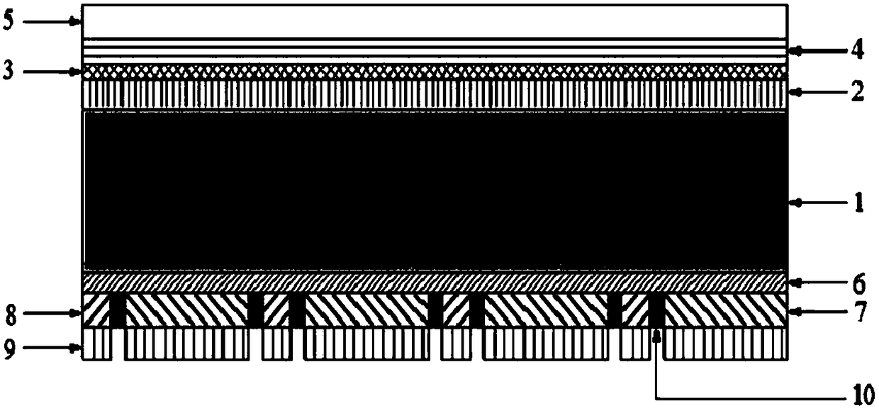
[0026] see figure 1 , is an interdigitated back-contact heterojunction monocrystalline silicon cell according to an embodiment of the present invention, and the monocrystalline silicon cell includes an N-type monocrystalline silicon substrate 1, wherein the N-type monocrystalline silicon substrate 1 has an opposite Front side and a back side; one side lightly doped N + Layer 2, amorphous silicon oxygen alloy (a-SiOx:H) front passivation layer 3, front N-type amorpho...


PUM

PropertyMeasurementUnit
Thicknessaaaaaaaaaa
Thicknessaaaaaaaaaa

Abstract

The invention discloses an interdigital back contact heterojunction monocrystal battery. The interdigital back contact heterojunction monocrystal battery comprises an N type monocrystal substrate, a doped N<+> layer and a front surface N type amorphous silicon layer arranged on the front surface of the N type monocrystal substrate, and a P type amorphous silicon layer and a back surface N type amorphous silicon layer arranged on the back surface of the N type amorphous silicon layer at intervals, wherein the N type monocrystal substrate comprises a front surface and a back surface which are opposite. According to the interdigital back contact heterojunction monocrystal battery disclosed in the invention, the thickness of the N type amorphous silicon layer on the front surface of the conventional back contact heterojunction N type monocrystal battery is thinned, and the lightly doped N<+> layer can be arranged below an amorphous silicon oxygen alloy layer, so that light absorption and light loss of the N type monocrystal layer can be lowered, and the photoelectric conversion efficiency of the battery can be improved by virtue of a partial field passivation function realized by the N<+> layer; and meanwhile, the N<+> layer also can provide transverse low-resistance conductive channels for photon-generated carriers, so that loss of a series resistor can be lowered, the short-circuit current of the battery can be reduced, and the filling factor and the conversion efficiency of the battery can be improved.

Description

technical field [0001] The invention relates to the technical field of solar cells, in particular to an interdigitated back-contact heterojunction single crystal silicon cell. Background technique [0002] Crystalline silicon solar cells have the characteristics of high conversion efficiency, good working stability, long working life and mature manufacturing technology, and are currently the main force in the solar photovoltaic market. Compared with the boron-doped P-type single crystal silicon material, the boron content in the phosphorus-doped N-type single crystal silicon material is extremely low, and the light-induced attenuation caused by the boron-oxygen pair can be ignored. The ability to capture holes is lower than that of impurities in P-type materials to minority electrons, and N-type silicon has a higher minority carrier lifetime than P-type silicon at the same doping concentration. These characteristics make N-type silicon cells have the advantages of potential...

Claims


Application Information

Patent Timeline
IPC IPC(8): H01L31/0216H01L31/0352H01L31/074
CPCH01L31/02167H01L31/02168H01L31/035272H01L31/035281H01L31/074Y02E10/50
Inventor 卢刚王海何凤琴郑璐钱俊杨振英王旭辉
Owner YELLOW RIVER PHOTOVOLTAIC IND TECH CO LTD
Why Eureka
Try Eureka