Photoelectric detector and preparation method thereof

A technology of photodetectors and gratings, applied in circuits, electrical components, semiconductor devices, etc., can solve problems such as increasing production costs, and achieve the effects of reducing production costs, enhancing feasibility, and simplifying production

Active Publication Date: 2019-07-05
HISILICON OPTOELECTRONICS CO LIMITED
View PDF9 Cites 10 Cited by
  • Summary
  • Abstract
  • Description
  • Claims
  • Application Information

AI Technical Summary

Problems solved by technology

[0004] Although figure 1 The light absorption region of the shown RCE detector structure is relatively thin, which is conducive to the rapid transfer of carriers to the electrode, but the epitaxy of the RCE detector structure requires a very thick DBR, and usually the thickness of the DBR can reach several microns, thereby increasing production cost

Method used


Image

  • Photoelectric detector and preparation method thereof
  • Photoelectric detector and preparation method thereof
  • Photoelectric detector and preparation method thereof

Examples


Embodiment 1

[0058] Embodiment 1, making a lower contact electrode on the lower contact layer;

[0059] Using metal-organic chemical vapor deposition (metal-organic chemical vapor deposition, MOCVD) technology or molecular beam epitaxy (MBE) technology, the buffer layer, lower contact layer, transition layer and absorption layer are epitaxially on the N-type substrate. Floor. If the remaining area is etched down to the lower contact layer, a lower contact electrode can be formed on the lower contact layer by a photolithography process.

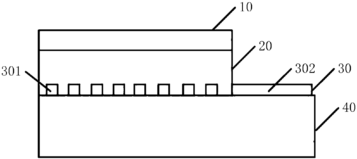
[0060] see figure 2 , figure 2 It is a schematic diagram of an embodiment of the photodetector in the embodiment of the present application, the photodetector includes an absorption layer 40, a metal layer 30, a dielectric film 20 and a reflective metal 10 arranged in sequence from the bottom layer to the top layer;

[0061] The absorbing layer 40 is used to absorb target detection light;

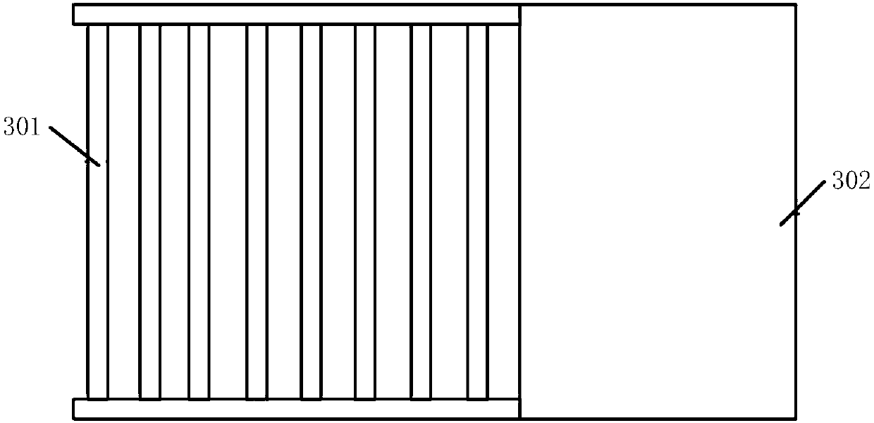
[0062] The metal layer 30 includes a strip grating 301 and a...

Embodiment 2

[0076] Embodiment 2, making the lower contact electrode on the N-type substrate;

[0077] Using MOCVD technology or MBE technology, the buffer layer, the transition layer and the absorption layer are extended sequentially on the N-type substrate. If the remaining area is etched to the N-type substrate, the lower contact electrode can be fabricated on the N-type substrate by photolithography.

[0078] see again figure 2 , figure 2 It is a schematic diagram of an embodiment of the photodetector in the embodiment of the present application, the photodetector includes an absorption layer 40, a metal layer 30, a dielectric film 20 and a reflective metal 10 arranged in sequence from the bottom layer to the top layer;

[0079] The absorbing layer 40 is used to absorb target detection light;

[0080] The metal layer 30 includes a strip grating 301 and an upper contact electrode 302. One side of the strip grating 301 is located on the absorbing layer 40. The strip grating 301 is u...


PUM


Abstract

The invention discloses a photoelectric detector, and the photoelectric detector comprises an absorption layer, a metal layer, a dielectric film and reflective metal, which are sequentially arranged from a bottom layer to a top layer. The absorption layer is used for absorbing target detection light. The metal layer comprises a strip-shaped grating and an upper contact electrode, and one side of the strip-shaped grating is located on the absorption layer, and the strip-shaped grating is used for gathering target detection light, and the upper contact electrode is electrically connected with alower contact electrode through a voltage. One side of the dielectric film is located above the other side of the strip-shaped grating, and the other side of the dielectric film is located below the reflective metal. The dielectric film is used for providing a cavity of the resonant cavity, and the reflective metal is used for reflecting target detection light. The invention also provides a preparation method of the photoelectric detector. According to the invention, a transverse resonant cavity effect and a longitudinal resonant cavity effect can be formed at the same time through the strip-shaped grating and the reflecting metal, and the higher light absorption rate is obtained in a thin absorption region. Moreover, the structure of the detector is simpler than the structure of a resonant cavity resonance detector, and the manufacturing cost is reduced.

Description

technical field [0001] The present application relates to the field of semiconductor devices, in particular to a photodetector and a method for preparing the photodetector. Background technique [0002] In the development of optical fiber communication system, photodetector is an indispensable part, and its performance plays a decisive role in the performance of the entire optical fiber communication system. The bandwidth of the photodetector and the quantum efficiency are mutually restricted. Generally, the quantum efficiency of the device can be increased by increasing the thickness of the absorbing layer of the photodetector. [0003] At present, a common photodetector is shown in 1, figure 1 It is a schematic diagram of a resonant cavity enhanced (RCE) detector in an existing solution. The RCE detector is integrated with a resonant cavity of a distributed Bragg reflection (distributed Bragg reflection, DBR) at both ends of an absorption region. When the light is incide...

Claims


Application Information

Patent Timeline
Patent Type & Authority Applications(China)
IPC IPC(8): H01L31/102H01L31/18
CPCH01L31/102H01L31/18Y02P70/50
Inventor 向伟郭敬书赵彦立曹均凯秦龙缪笛
Owner HISILICON OPTOELECTRONICS CO LIMITED
Why Eureka
Try Eureka