LED epitaxial growth method for reducing warping

An epitaxial growth and warping technology, applied in electrical components, circuits, semiconductor devices, etc., can solve the problems of large warpage and high fragmentation rate of epitaxial wafers, and achieve surface hexagonal defects and concave pits, good appearance, smooth surface Effect

Active Publication Date: 2019-07-05
XIANGNENG HUALEI OPTOELECTRONICS
View PDF6 Cites 0 Cited by
  • Summary
  • Abstract
  • Description
  • Claims
  • Application Information

AI Technical Summary

Problems solved by technology

[0005] In view of this, the present invention provides an LED epitaxial growth method with reduced warpage, which solves the technical problems of

Method used


Image

  • LED epitaxial growth method for reducing warping
  • LED epitaxial growth method for reducing warping
  • LED epitaxial growth method for reducing warping

Examples


Embodiment 1

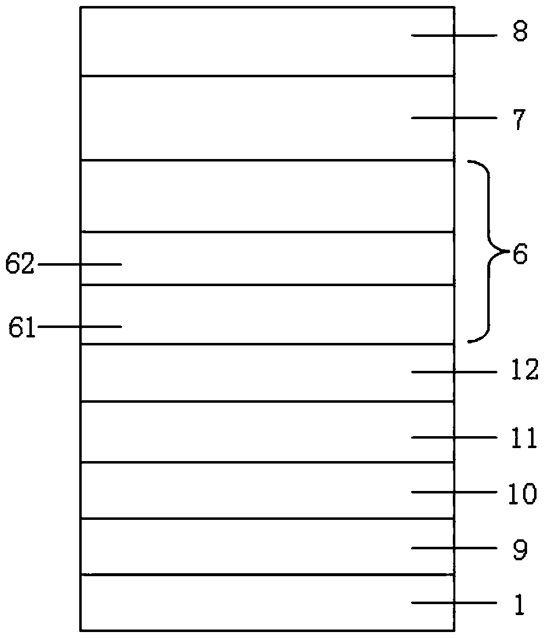
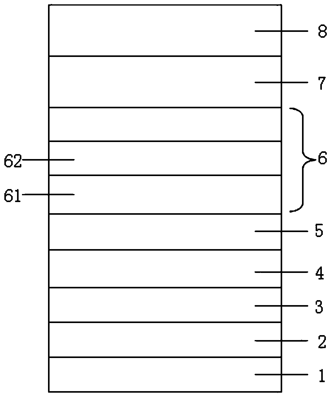
[0042] The epitaxial layer structure is as figure 1 shown. The present invention uses MOCVD (metal organic compound chemical vapor deposition) to grow LED epitaxial wafers, using high-purity H 2 or high purity N 2 or high purity H 2 and high purity N 2 The mixed gas as the carrier gas, high-purity NH 3 As the N source, the metal-organic source trimethylgallium (TMGa), triethylgallium (TEGa) is used as the gallium source, trimethylindium (TMIn) is used as the indium source, and the N-type dopant is silane (SiH 4 ), trimethylaluminum (TMAl) as the aluminum source, and the P-type dopant as magnesium dicene (CP 2 Mg), the substrate is a sapphire substrate, the reaction pressure is between 70mbar and 900mbar, and the specific growth method is as follows:

[0043] A method for reducing warpage of LED epitaxial growth, comprising: processing substrate 1, growing Al z Ga 1- z N layer 2, growing AlN layer 3, growing MgAl y Ga 1-y N layer 4, growth of Si-doped N-type GaN laye...


PUM

PropertyMeasurementUnit
Thicknessaaaaaaaaaa

Abstract

The invention discloses an LED epitaxial growth method for reducing warping. The method comprises the following steps of processing a substrate; growing an AlzGa1-zN layer, an AlN layer, a MgAlyGa1-yNlayer, a Si-doped N-type GaN layer, an InxGa(1-x)N/GaN light-emitting layer, a P-type AlGaN layer and a magnesium-doped P-type GaN layer; and performing temperature reduction and cooling, wherein x is equal to 0.20-0.25. The LED epitaxial growth method solves the technical problem in the prior art that the LED epitaxial wafer has large warpage and high fragmentation rate, and makes the surface appearance of the epitaxial wafer better.

Description

technical field [0001] The present application relates to the technical field of LED epitaxial design application, in particular, to an LED growth method for reducing warping of epitaxial wafers. Background technique [0002] LED (Light Emitting Diode, Light Emitting Diode) is a kind of solid-state lighting. Due to the advantages of LED, such as small size, low power consumption, long service life, high brightness, environmental protection, and durability, it is recognized by consumers, and the scale of domestic LED production is also increasing. Gradually expand. [0003] Sapphire is the most common substrate material for industrial growth of GaN-based LEDs at this stage. In the current traditional epitaxial growth technology, the warpage of the epitaxial wafer is large, especially when the epitaxial crystal is grown on a large-sized sapphire substrate, the warpage is even greater, resulting in a high rate of grinding fragments in the subsequent chip manufacturing process ...

Claims


Application Information

Patent Timeline
IPC IPC(8): H01L33/00H01L33/12H01L21/67
CPCH01L33/007H01L33/12H01L21/67248H01L21/67253
Inventor 徐平
Owner XIANGNENG HUALEI OPTOELECTRONICS
Why Eureka
Try Eureka