Semiconductor device

A semiconductor and bipolar transistor technology, which is applied in the fields of semiconductor devices, semiconductor/solid-state device manufacturing, electric solid-state devices, etc., and can solve problems such as difficulty in manufacturing yields

Active Publication Date: 2019-07-09
MURATA MFG CO LTD
View PDF14 Cites 0 Cited by
  • Summary
  • Abstract
  • Description
  • Claims
  • Application Information

AI Technical Summary

Problems solved by technology

[0006] According to the investigation of the inventors of the present application, it is found that it is difficult to secure a sufficient manufacturing yield in order to provide the HBT disclosed in Patent Document 1 as a device for high-frequency power amplifiers.

Method used


Image

  • Semiconductor device
  • Semiconductor device
  • Semiconductor device

Examples


no. 1 example

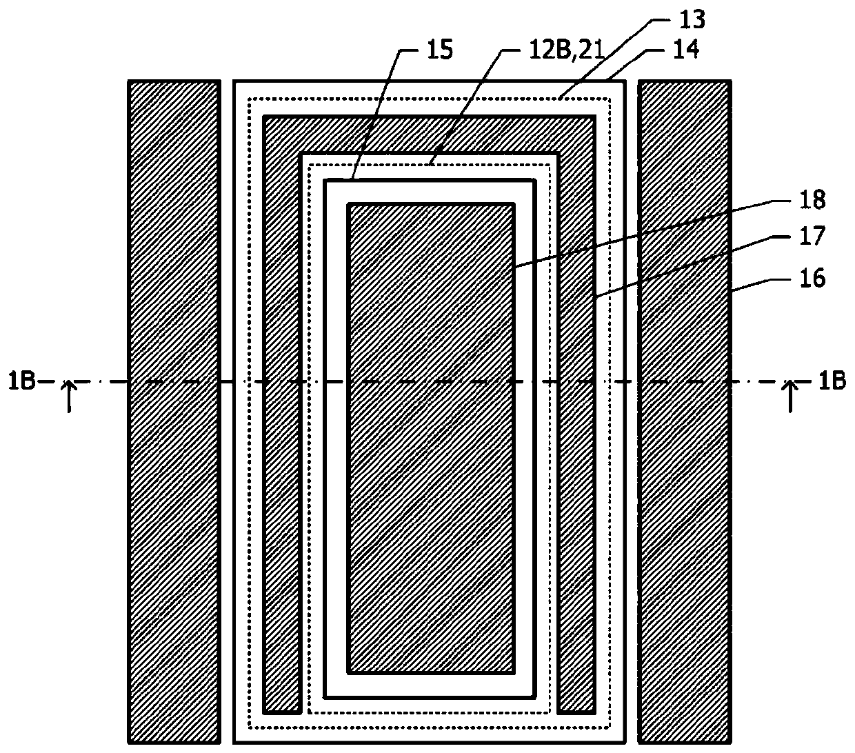
[0092] Next, refer to Figure 1A as well as Figure 1B , the semiconductor device of the first embodiment will be described.

[0093] Figure 1A is a plan view of the semiconductor device of the first embodiment, Figure 1B Yes Figure 1A The sectional view of the dotted line 1B-1B.

[0094] On a substrate 10 made of a semiconductor, a sub-collector layer 11 made of an n-type semiconductor is epitaxially grown. On the sub-collector layer 11, the collector layer 12 made of n-type semiconductor, the base layer 13 made of p-type semiconductor, the emitter layer 14 made of n-type semiconductor, and the Emitter contact layer 15. The collector layer 12 is arranged on a part of the sub-collector layer 11 .

[0095] The collector layer 12 includes a first collector layer 12A on the substrate side and a second collector layer 12B thereon. The composition of the first collector layer 12A is different from that of the second collector layer 12B, and the etching characteristics of th...

no. 2 example

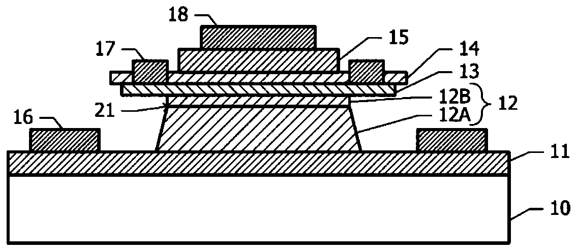
[0110] Next, refer to Figure 2 ~ Figure 3J The accompanying drawings describe the semiconductor device of the second embodiment. Below, for the first embodiment ( Figure 1A , Figure 1B ) The description of the same configuration as the semiconductor device is omitted.

[0111] figure 2 is a cross-sectional view of the semiconductor device of the second embodiment. In the second embodiment, an etching stopper layer 22 is disposed between the sub-collector layer 11 and the first collector layer 12A. Etching stopper layer 22 has an etching characteristic different from those of first collector layer 12A and sub-collector layer 11 . In a plan view, the edge of the upper surface of the etching stopper layer 22 is arranged on the inner side than the edge of the lower surface of the first collector layer 12A.

[0112] The conductivity type of the etching stopper layer 22 is the same as that of the sub-collector layer 11 , and the doping concentration of the etching stopper l...

no. 3 example

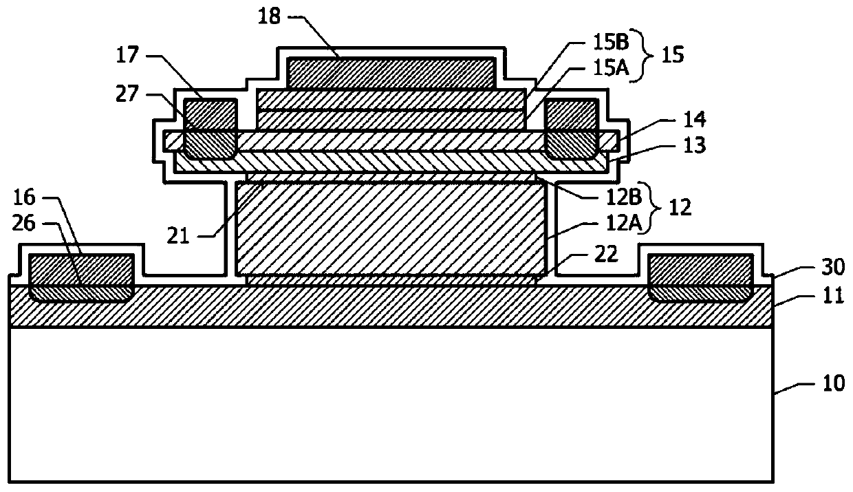
[0148] Next, refer to Figure 4A as well as Figure 4B , the semiconductor device of the third embodiment will be described. Hereinafter, for the semiconductor device of the second embodiment ( figure 2 ) with the same configuration is omitted.

[0149] In the second embodiment, the second collector layer 12B ( figure 2 ) uses InGaP, but in the third embodiment, InGaPN is used. The molar ratio of In to Ga is 0.528:0.472, and the molar ratio of P to N is 0.995:0.005. At this time, the electron affinity of the second collector layer 12B is almost equal to the electron affinity of the base layer 13 made of GaAs. In the third embodiment, the doping concentration of the second collector layer 12B is also the same as that of the second collector layer 12B of the semiconductor device of the second embodiment.

[0150] Figure 4A as well as Figure 4B are the semiconductor devices of the third embodiment and the second embodiment ( figure 2 ) energy band diagrams of the ba...


PUM

PropertyMeasurementUnit
thicknessaaaaaaaaaa
thicknessaaaaaaaaaa
thicknessaaaaaaaaaa

Abstract

Provided is a semiconductor device capable of improving gain in a high frequency band and suppressing a decrease in manufacturing yield. A bipolar transistor including a first collector layer, a second collector layer, a base layer, and an emitter layer is disposed on a substrate. Etching characteristics of the second collector layer are different from etching characteristics of the first collector layer and the base layer. In plan view, an edge of an interface between the first collector layer and the second collector layer is disposed inside an edge of a lower surface of the base layer, andan edge of an upper surface of the second collector layer coincides with the edge of the lower surface of the base layer or is disposed inside the edge of the lower surface of the base layer.

Description

technical field [0001] The present invention relates to semiconductor devices. Background technique [0002] Now, mobile communication systems represented by mobile phone terminals are moving from the fourth generation (4G) to the fifth generation (5G). In the fifth generation mobile communication system, a higher frequency band is used than in the fourth generation mobile communication system. As the frequency increases, the power loss of the high-frequency circuit also increases, so there is an increasing demand for a higher gain of the high-frequency power amplifier, which is a main component of a mobile phone terminal for the fifth-generation mobile communication system. High frequency power amplifiers generally use heterojunction bipolar transistors (HBT). [0003] There is known an HBT in which base-collector capacitance is reduced in order to improve high-frequency characteristics (for example, Patent Document 1). The HBT disclosed in Patent Document 1 includes a c...

Claims


Application Information

Patent Timeline
Patent Type & Authority Applications(China)
IPC IPC(8): H01L29/08H01L29/737
CPCH01L29/7371H01L29/0821H01L21/30612H01L21/30617H01L29/205H01L29/0826H01L29/42304H01L29/1004H01L29/66318H01L2224/13082H01L24/13H01L2224/05572H01L2224/05027H01L2224/05022H01L2224/13147H01L2224/13139H01L2224/13111H01L2224/05647H01L2224/05166H01L2224/05144H01L2224/0518H01L2224/05169H01L2924/00014H01L2924/014H01L2924/0105H01L2924/01047H01L29/0817H01L21/02538H01L21/0262H01L21/28575H01L21/308H01L29/66242H01L2224/13025H01L2224/13083H01L2224/13166
Inventor 大部功梅本康成柴田雅博小屋茂树近藤将夫筒井孝幸
Owner MURATA MFG CO LTD
Why Eureka
Try Eureka